
Computer memory power supply circuit NCP5201

The NCP5201 is a highly integrated power management solution designed specifically for memory applications. This chip can deliver two distinct output voltages, which are essential for powering different types of memory modules, such as DDR and DDR2 RAM. The dual-output capability allows for optimized performance by supplying the necessary voltages required by each memory type, ensuring efficient operation and stability.
The circuit typically includes input capacitors to filter the power supply voltage, ensuring a stable input to the NCP5201. Output capacitors are also essential for smoothing the output voltages and providing transient response during load changes. The feedback loop is implemented using resistors that set the output voltage levels, which can be adjusted according to the specific requirements of the memory modules being powered.
The NCP5201 also features integrated protection mechanisms such as over-voltage protection (OVP) and under-voltage lockout (UVLO), which safeguard the memory components from potential damage due to voltage fluctuations. Additionally, the chip can support various switching frequencies, allowing for flexibility in design and optimization for efficiency.
In summary, the computer memory power supply circuit utilizing the NCP5201 is a robust solution for powering memory modules, featuring dual outputs, integrated protection features, and adjustable voltage settings, making it an ideal choice for modern computer systems.Computer memory power supply circuit (NCP5201) It shows a typical computer memory power supply circuit. The circuit is a dual-output circuit, NCP5201 power management chip,
Related Circuits
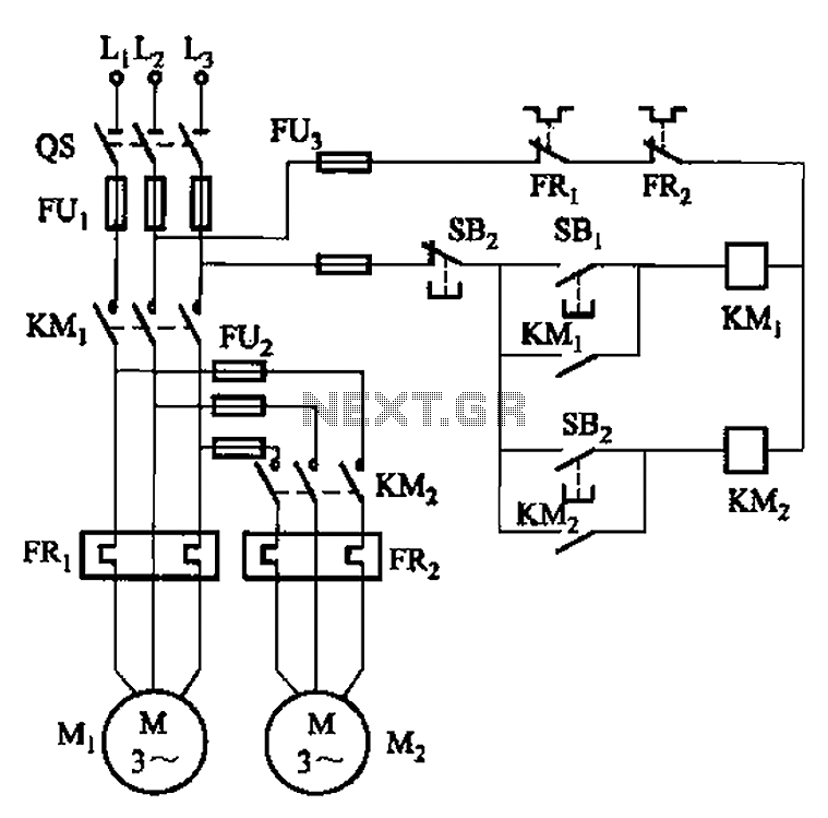
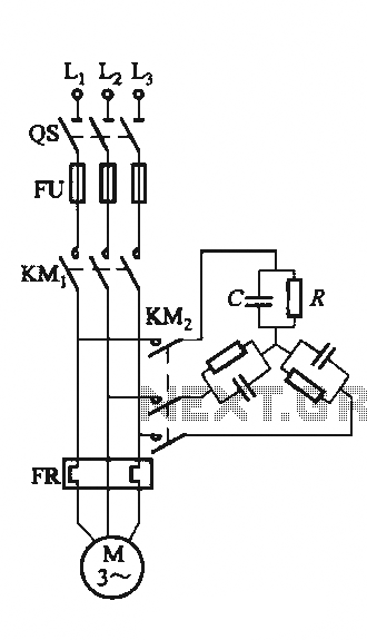
The circuit illustrated in Figure 3-83 demonstrates that the contactor KMi is activated only after it is pulled, which indicates that the motor Mi has started for the first time. Following this, the contactor KM2 is then activated, indicating...
Most universal radio receivers have a very wide bandwidth that is not particularly suitable for radio amateurs. The better models with narrower bandwidth are almost a... Universal radio receivers are designed to operate over a broad frequency range, making them...
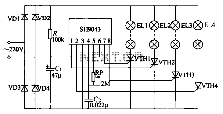
This example demonstrates a robust design featuring novelty lights that flash in a specific sequence, utilizing a 1-3-2-4 vault chase mode. The circuit includes diodes VD1 to VD4, which form a bridge rectifier, converting AC voltage to a full-wave...
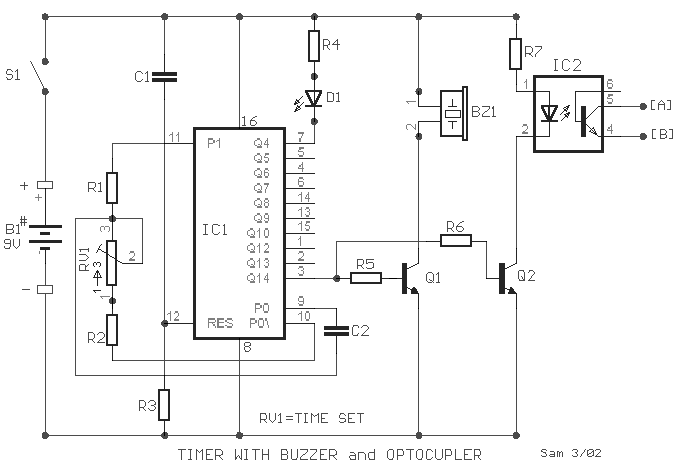
A small circuit designed for various time measurement applications. It features an audible sound signal from the buzzer BZ1 and has the capability to drive an external circuit through the optocoupler IC2, once the appropriate circuit is connected to...
The circuit illustrated in Figure 3-151 consists of capacitor banks arranged in a specific configuration. Figure 3-151 (a) depicts capacitor banks connected in a shaped configuration, which is suitable for shaped or Y-connected motors. Figure 3-151 (b) shows Y-connected...
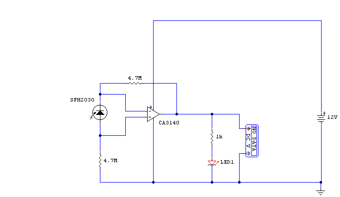
While developing an infrared (IR) extender circuit, a method was needed to measure the relative intensities of different infrared light sources. This circuit utilizes an SFH2030 photodiode as the infrared sensor. A CA3140 MOSFET operational amplifier is employed in...