
Computer Power Supply
The switch mode power supply (SMPS) operates through several key stages, starting with the AC input, which is filtered by the EMI filter to eliminate noise and comply with regulations. Following this, the rectifier bridge converts the AC voltage to DC, and the PFC stage enhances the power factor, ensuring efficient energy usage. The boost converter raises the voltage to a level suitable for the power transformer, which is crucial for the subsequent DC-DC conversion stage.
The primary transformer (T1) in the forward converter design serves to isolate the input from the output while stepping down or stepping up the voltage as needed. The switching action of Q2 is controlled by a PWM signal, which regulates the output voltage by adjusting the duty cycle of the switching device. This allows for efficient energy transfer and minimizes losses during operation.
The output stage typically includes additional filtering to smooth the DC output, ensuring that the voltage supplied to the load is stable and within specified limits. The rectifier diodes convert the transformed voltage back to DC, which is then provided to the connected load. The design of the SMPS allows for compact construction and high efficiency, making it suitable for a wide range of applications, from personal computers to industrial equipment.
In conclusion, the SMPS is a critical component in modern electronic systems, providing reliable power conversion while adhering to strict regulatory standards for performance and efficiency. Understanding its operation and components is essential for anyone involved in the design, integration, or troubleshooting of electronic systems.All electronic systems and equipment regardless of their size or function have one thing in common: they all need a power supply unit (PSU) that converts input voltage into a voltage or voltages suitable for their circuits. The most common type of today`s PSU is the switch mode power supply (SMPS). There is a wide variety of SMPS topologies and th eir practical implementations used by PSU manufacturers. However they all use the same basic concepts. This page explains the principals of operation of a switching mode power supply and reviews its main parts and functions. This tutorial can be useful for system integrators, hobbyists, and those who are not necessarily experts in power electronics.
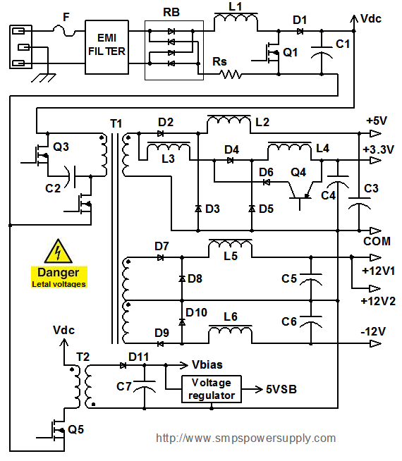
This is a conceptual circuit diagram of the power train of a typical ATX computer power supply unit. This schematic does not show the control circuitry, that`s why you see all MOSFET gates and transistor bases are open. For clarity, the parts responsible for miscellaneous auxiliary functions, such as current limit, fan control, and OV protection, which are not essential for learning the basic concepts of the power conversion, are not shown as well.
For a complete schematic, see for example this annotated diagram of an ATX power supply. Note that unlike generators that convert energy stored in various fuels into electricity, PSUs convert electric energy from one form to another. The AC input receptacle in a PC is an IEC 320 type or equivalent. The fuse "F" is followed by an EMI filter. The filter is normally consists of a combination of differential mode and common mode chokes and capacitors.
Its main purpose is to reduce the conducted radio frequency noise emitted from the power supply back into the input line to comply with regulatory requirements. Reducing conducted noise also reduces radiated emissions from the input power lines that act as an antenna.
The input section usually also includes inrush current limiting and surge protecting components. The EMI filter in most off-line SMPS PSU is followed by a rectifier bridge (RB) and a power factor correction (PFC) stage. This stage was absent from older SMPS, in which the rectifier was followed by a large storage capacitor.
Power supply manufacturers began introducing PFC technique beginning late 80`s when Europeans introduced EN61000-3-2 norm. This document specifies the maximum amplitude of line-frequency harmonics for various categories of equipment.
Our diagram shows a typical PFC stage that consists of a full-wave rectifier and boost converter with a storage capacitor C1. Note that in this scheme the current always flows through two diodes of the rectifier bridge. There are also so-called bridgeless PFC which eliminate one diode from the current pass. The storage capacitor is designed to provide energy to the output during short input power interruptions.
In practice, there may be several paralleled storage caps. The computer power supplies as well as commercial units normally have to ride through at least one cycle of input sine wave, which is 16 ms in U. S. and 20 ms in Europe. The PFC boost provides DC-link voltage (Vdc) which is higher than the peak of input AC. In modern computer PSU, this voltage is typically 375-400 VDC. If you are trying to troubleshoot a unit and you measure about 160VDC across C1- it means the boost stage does not work.
The output DC-DC stage in any SMPS always contains one or more switching devices that periodically commutate LC networks. The above diagram shows a so-called forward converter with active reset. Half-bridge is also often used in the PC designs. See examples of schematics based on half-bridge: 250W and 300W. The main switch Q2 periodically applies voltage Vdc to the primary of power transformer T1. When Q2 is in "on" state, positive voltage appears at the upper terminals of the T2 secondaries. As the result, rectifier diodes D2, D4, D7 and D9 conduct, and the energy from the inp 🔗 External reference
Related Circuits
Currently, a basic MOSFET amplifier or power amplifier is designed to deliver an output power of ±100 Watts RMS with an 8 Ohm load, or ±160 Watts RMS with a 4 Ohm load. The simplicity of this circuit results...
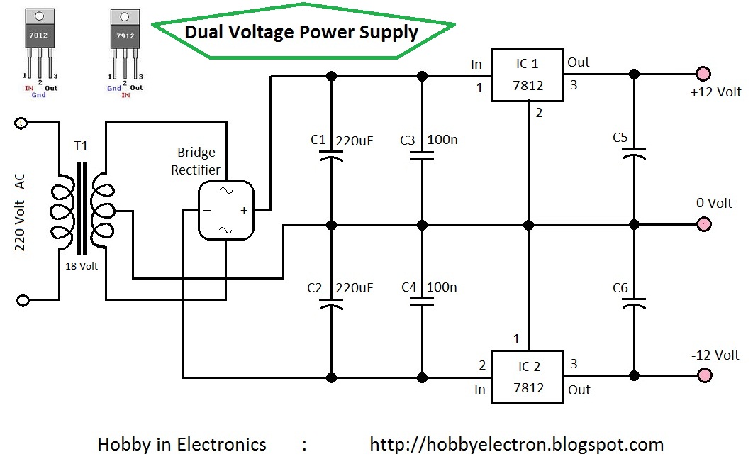
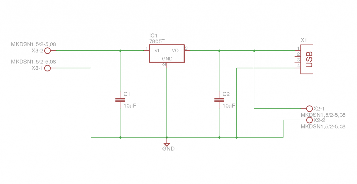
Circuit Home 7809 7812 7909 7912 Dual Voltage Hobby Electronics Hobby electronics projects RC filters REGULATOR transformer Dual Voltage Power Supply 12 Volt This is the simple circuit diagram of a Dual Voltage Power Supply. It is used for...
This device enables remote control of AC-powered appliances by utilizing the beam of a flashlight as a triggering mechanism. A key feature of this gadget is its memory function; activating it once supplies power to the device, and it...
This document outlines the details of several circuits designed and built for a robot. The first circuit is a voltage regulator intended to supply power to a Raspberry Pi from a 7.2V battery. While the circuit is relatively simple,...
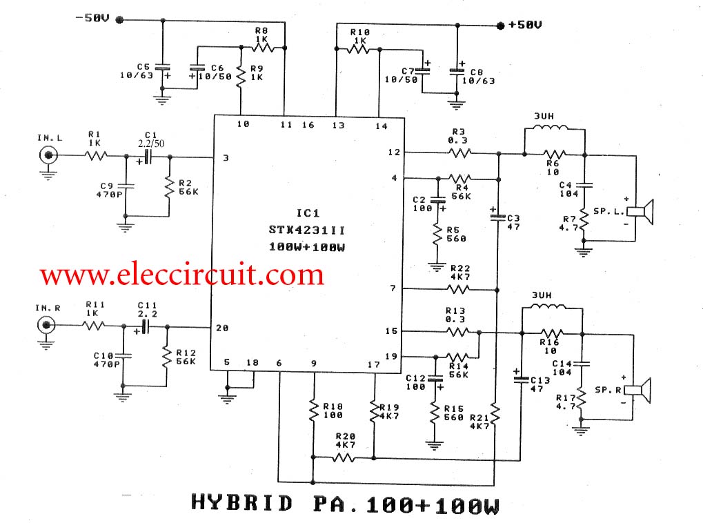
To create a 100-watt OCL audio amplifier circuit, consider using this design. It incorporates the STK4231 integrated circuit, which is a compact and cost-effective solution. The STK4231 is a hybrid IC from Sanyo, belonging to the STK4201II series, capable...
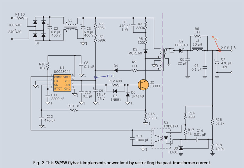
Through simple circuit modifications, designers can use peak current limiting to produce a constant current source. A constant current source is an essential component in various electronic applications, providing a steady output current regardless of load fluctuations or variations in...
Warning: include(partials/cookie-banner.php): Failed to open stream: Permission denied in /var/www/html/nextgr/view-circuit.php on line 713
Warning: include(): Failed opening 'partials/cookie-banner.php' for inclusion (include_path='.:/usr/share/php') in /var/www/html/nextgr/view-circuit.php on line 713