
converter voltmeter to frequency meter

The circuit design effectively integrates multiple stages to achieve voltage-to-frequency conversion, making it suitable for applications in automotive and industrial environments. The squarer stage ensures that the input signal is appropriately conditioned, protecting sensitive components from high voltage levels. The inclusion of a Zener diode for voltage spike protection further enhances the reliability of the circuit.
In the second block, the use of a retriggerable monostable multivibrator allows for precise control over pulse width, which is critical in applications requiring accurate frequency measurement. The calculated pulse widths and their corresponding output voltages demonstrate the versatility of the design, accommodating a wide frequency range and allowing for easy calibration to different engine types.
The low-pass filter in the final block smooths the output signal, ensuring that the voltage readings remain stable and free from high-frequency noise, which is essential for accurate tachometer readings. The recommendation to include a decoupling capacitor highlights the importance of noise management in sensitive electronic circuits.
Overall, the circuit is well-structured to provide reliable voltage-to-frequency conversion, making it a valuable tool for speed sensing and tachometric applications across various fields.This is design circuit for converter meter voltage to frequency. Normally we often encountered the frequency meter can be used in speed sensor, tachometer, measurement or signal recurring. This frequency to voltage converter (FVC) can be used to change the voltage into a digital or analog tachometer.
Circuit that is consists of three blocks. The f irst block is squarer, the input signal to a square wave. This block was protected the circuit from high input voltage up to 400V, but remember this only works if the value of capacitor C1 is for 400V. Input Impedance around 560k, so it is safe to connect the ignition pick-up coil in parallel with the CDI (capacitor discharge ignition) circuits without a problem.
Supply is protected from voltage spike by Zener diode D3. This is the figure of the circuit; The second block is retriggerable mono stable multi vibrator. Mono stable multi-vibrator is to convert fixed width pulses to provide output, the voltage output of the average will depend on the duty factor pulses input / waveform, but only depends on the input frequency. Pulse width is determined by R9 + R5 and C4. According to the datasheet of IC 4528, the period of the mono stable : R and C are in ohm and Farad, VDD-VSS is in the pin 16 voltage minus the voltage on pin 8, and t in seconds.
Minimal value of R9, the mono stable multi-vibrator output pulse width will be 0. 2 * 4700 * 22e-9 * ln (12) = 5. 139e-5, and this will change the frequency of 19. 460 kHz to 12 Volt output. This gives a conversion factor 1. 622kHz/Volt. If you set the maximum value to R9 (100k) then the pulse width of mono stable multi-vibrator output will 1. 145 MS. This setting will give the maximum voltage output of 12V at 874Hz, or about 72. 8Hz per Volt conversion. If you use the tachometer to the application, wide rage this adjustment will accommodate almost any type of engine.
A last block of the first order low pass filter about U2, about 0. 1 seconds of time set by R6 and C5 constant. With the slow time, you can not read all the frequencies below 10Hz or close, but OK for a variety of applications. Although the diagram does not show the scheme decoupling capacitor for bypassing the supply line for u3 noise, it`s good to add a 100nF cap u3 as close as possible to the power pin (pin 8 and 16), since the mono stable multi-vibrator is sensitive to such noise.
🔗 External reference
Related Circuits
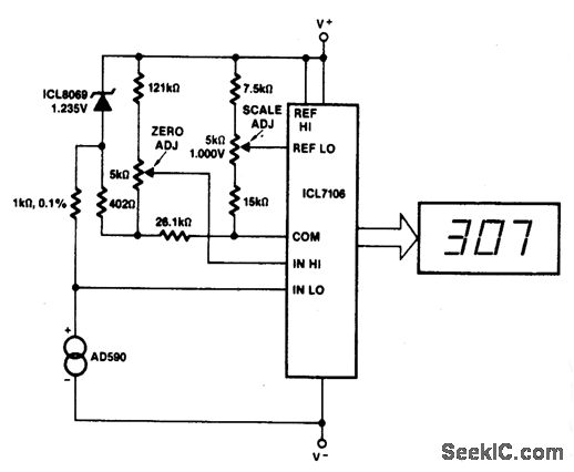
This circuit allows for zero adjustment as well as slope adjustment. The ICL8069 brings the input within the common-mode range, while the 5 K pots trim any offset at 218 °K (-55 °F) and set the scale factor. The...
The LM35 from National Semiconductor is a precision centigrade temperature sensor that provides an analog output voltage. It operates within a temperature range of -55°C to +150°C and has an accuracy of ±0.5°C. The output voltage corresponds to 10mV...
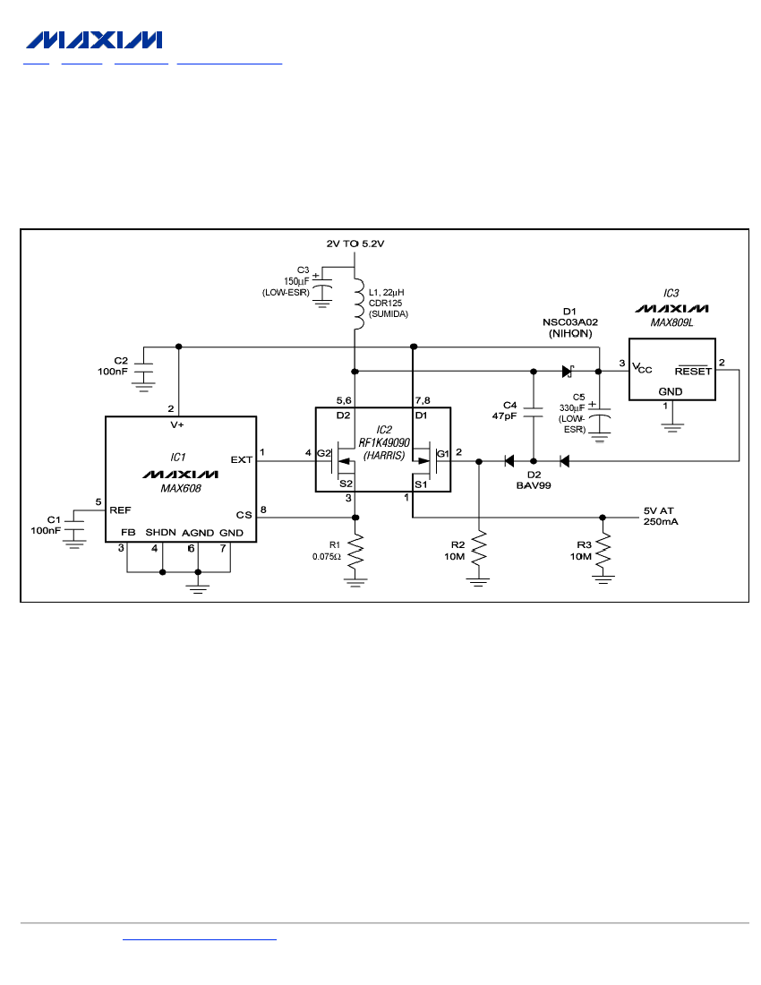
To ensure a full-load start-up, the additional circuitry in this regulated boost converter disconnects the load until the output voltage reaches regulation. Proper operation necessitates a gate-drive voltage adequate to maintain low on-resistance in the switching MOSFET; however, during...
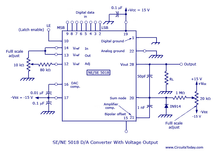
Monolithic and hybrid digital-to-analog converters utilizing MC 1408 IC and SE/NE 5018, including specifications and applications. Digital-to-analog converters (DACs) are integral components in various electronic systems, enabling the conversion of digital signals into corresponding analog voltages or currents. The MC...
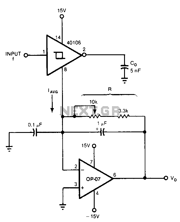
Six components can configure a circuit whose output voltage is proportional to its input frequency. The average current from the ground pin 8 of the 40106 Schmitt trigger inverter is linearly dependent on the frequency at which the capacitor...
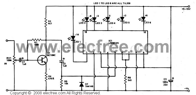
This is an LED VU Meter circuit using the LM3914 IC, designed to visually represent audio signals in stereo or sound applications. The circuit is straightforward to assemble, utilizing a single integrated circuit (IC) to display 10 levels of...