
Cortex M3 MCU features USB firmware protection

6 2V core voltage. When asked what differentiates Atmel from the other Cortex competitors, Product Marketing Manager Jacko Wilbrink offered this assesment: "The majority of other Cortex M3-based devices are targeted to low and mid-level data rate applications. We have built an ARM9-type infrastructure around our M3 core, with lots of DMA options, multilayer busses and segmented memories that can support high-end communication from high speed USB, SDIO, MMC and SPI.
" Atmel used their experience designing high speed USB for their SAM9 product line and have been able to port the design to the lower power, lower speed Cortex-M3. (For some more technical details on how they were able to do it, read this article ) The SAM3U is currently the only Cortex-M3 design to offer high speed USB.
Building on their experience with high speed interfaces in general, the SAM3U also contains SDIO/SD/MMC host and SPI interfaces on-chip. Borrowing from Atmel`s experience in smart card market, the SAM3U also features an on chip memory protection unit (MPU) and a 128-bit unique ID (for every device) that both can be used to protect the firmware both on-chip, and in an external memory device.
As more resources get poured into firmware developement than hardware, protecting the algorithms that make the system work becomes more important. The added security might be just enough to dissuade a potential counterfeiter. The device also has a high data-bandwidth architecture with a 5-layer bus matrix, 23 DMA channels and distributed on-chip memory including up to 52Kbytes of SRAM split into three blocks and up to 256Kbytes of flash in two banks.
The dual bank flash offers in-application programming (IAP) where one memory bank is written with a new version of the firmware while the processor executes from the other bank. A programmable boot feature enables switching between the two flash banks at the next MCU reboot. Additional features include 12- and 10-bit ADCs, 5 UARTs, dual I2C, I2S, timers, and power and reset management.
The SAM3U`s supply voltage ranges from 1. 62 to 3. 6V. The SAM3U is aimed at applications such as high speed gateways in industrial, medical, data processing and telecom. The SAM3U flash MCU has a maximum clock rate of 96 MHz at 1. 8V, 85 °C and integrates high data rate peripherals including a 480 Mbps high-speed USB device, 384 Mbit/s 1/4/8-bit MMC 4.
3 Host, 192 Mbps 1/4-bit SDIO/SDCard 2. 0, 48 Mbit/s SPI, a 1Msample/s 12-bit ADC and a 500+ Mbps external bus interface. A combination of a 5-layer system bus matrix, dual peripheral bus, 4 central DMA channels, one dedicated DMA to the high speed USB device, 17 Peripheral DMA (PDC) channels, and distributed memory of up to 52Kbytes of SRAM split in three blocks and 256Kbytes of flash in two banks ensures uninterrupted internal and external data flows with minimum processor overhead. The central DMA features a built-in FIFO for increased tolerance to bus latency, programmable length burst transfers that optimize the average number of clock cycles per transfer, scatter, gather and linked list operations.
It can be programmed for memory-to-memory transfers or memory-to-peripheral like a high speed SPI or SDIO/SD/MMC media card interfaces (MCI). The high speed DMAs have a dedicated layer in the bus matrix for parallel data transfers. The peripheral DMA isintegrated in the peripheral programmer`s interface and has a reduced linked list support, limited to two memory areas.
The SAM3U is able to simultaneously stream several 100Mbit/s peripherals, process the payload and control the syst 🔗 External reference
Related Circuits
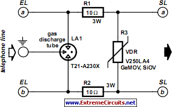
A long time ago, when telephones were simple and reliable from an electrical standpoint, telecom operators installed surge protection on all telephone lines exposed to storm risks. Ironically, this protection has diminished as more delicate and expensive equipment, such...
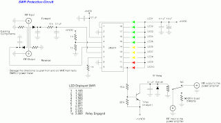
This document outlines a simple SWR (Standing Wave Ratio) protection circuit that can be easily constructed. The directional coupler and detector components are sourced from an old VHF SWR meter. It is advisable to replace the existing RF bypass...
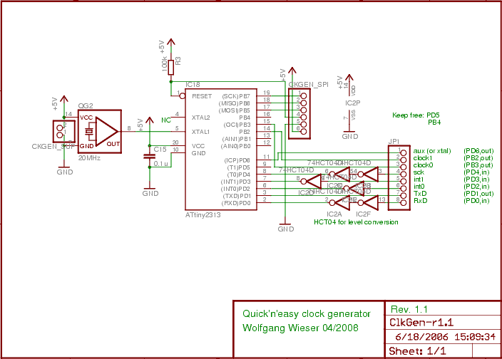
The design generates varying sampling clock write strobe pulses using an ATtiny2313 microcontroller from Atmel. For a 10MHz sampling clock, a 20MHz clock is required for the ATtiny2313, necessitating a power supply of 5V instead of 3.3V, which is...
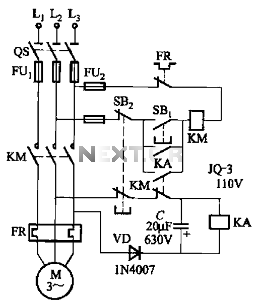
The circuit illustrated in Figure 3-73 is designed to utilize the power generated by instantaneous power failures, specifically the self-induced electromotive force (emf) produced by the motor, to implement an immediate shutdown protection mechanism. During a momentary power outage,...
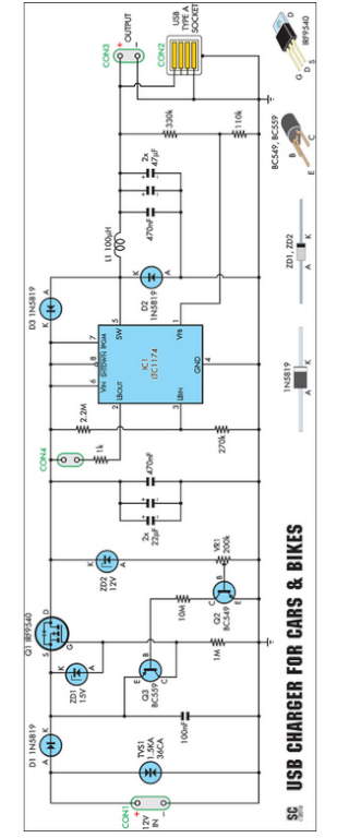
Seeking an efficient USB charger capable of operating from a 12V car battery? This unit operates at up to 89% efficiency and can charge USB devices effectively. This USB charger circuit is designed to convert a 12V car battery supply...
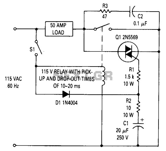
This circuit can be utilized to prevent relay contact arcing for loads up to 50 amperes. A delay exists between the moment a relay coil is energized and when the contacts close, as well as a delay from when...