
Create a flash-then-steady LED using a 555 timer

Additionally, the inclusion of resistor R2, capacitor C2, and transistor Q1 facilitates a delayed reset, causing LED1 to flash before remaining on continuously. The operation of the circuit is as follows: upon powering up (when VCC is applied), capacitor C2 is initially discharged, Q1 remains off, and reset pin 4 is at VCC. The circuit operates in astable mode, and capacitor C1 begins charging through resistors RA and RB. When the voltage across C1 (V6) reaches 2/3 VCC, C1 starts discharging through RB. Once V6 decreases to 1/3 VCC, C1 begins to charge again. This oscillation causes the voltage across C1 to fluctuate between 2/3 and 1/3 VCC, during which time LED1 continues to flash. Concurrently, capacitor C2 charges through R2 towards VCC. The diodes D1, D2, D3, and the base-emitter junction of Q1 provide a turn-on voltage (VR) of 2 V. When the voltage across C2 (VC2) reaches VR, Q1 activates and resets the timer. Consequently, the output voltage (V3) drops low, and LED1 remains illuminated until the power is disconnected. If the LED is connected between pin 3 and ground, it will flash and subsequently turn off. The initial charging time (ts) required for C1 to charge from 0 to 2/3 VCC can be calculated using standard timing equations. This LED driver circuit, which effectively captures attention through flashing, is widely applicable in front-panel indicators on various instruments, such as spectrum analyzers, oscilloscopes, signal sources, as well as in power-on indicators, warning lights, and laser pointers.
The circuit employs the 555 timer IC in its astable configuration, which allows continuous oscillation between two voltage levels. The timing components, RA and RB, determine the frequency of the oscillation, while the timing capacitor C1 sets the duration of the high and low states. The addition of R2 and C2 introduces a delay mechanism that allows for the initial flashing of the LED before it remains on, enhancing the circuit's functionality. The transistor Q1 serves as a switch that resets the timer, ensuring that the LED remains lit after the initial flash. The use of diodes helps in controlling the voltage levels and ensuring proper operation of the reset function.
This circuit can be optimized by selecting appropriate values for RA, RB, C1, R2, and C2 to achieve the desired flashing frequency and duration. The design can also be adapted for various applications by modifying the component values or integrating additional features such as adjustable brightness or multiple LEDs. Overall, this versatile circuit design illustrates the practical use of the 555 timer in creating attention-grabbing LED indicators suitable for a wide range of electronic devices.The circuit shown flashes the LED briefly (to get your attention) and stays on as long as the power is on ( Fig. 1 ). The venerable 555 timer IC can be put to use in this type of application. The circuit is a standard astable multivibrator with resistors RA, RB, and the timing capacitor C1. To operate as a free-running astable, the reset pin 4 should be held at VCC to disable reset. With the addition of R2, C2, and Q1, a delayed reset occurs that makes LED1 flash and then remain on. The circuit functions as follows: At the instant VCC is turned on, C2 is fully discharged, Q1 is off, and reset pin 4 is at VCC.
The circuit operates as an astable and C1 begins to charge through RA and RB. Once V6 reaches 2/3 VCC, C1 begins to discharge through RB. Once V6 reaches 1/3 VCC, the capacitor begins to charge again. The voltage across C1 oscillates between 2/3 and 1/3 VCC ( Fig. 2 ). During this time LED1 continues to flash. Meanwhile, C2 charges through R2 toward VCC. The diodes D1, D2, D3, and VBE (Q1) provide a turn-on voltage (VR) of 2 V. Once VC2 reaches VR, Q1 turns on and resets the timer. The output voltage V3 goes low and LED1 stays on until the power is turned off. If the LED is connected between pin 3 and ground, it will flash and stay off. The starting charging time (ts) to charge C1 from 0 to 2/3 VCC is: This attention-grabbing LED driver circuit finds numerous applications in frontpanel LEDs on instruments (such as spectrum analyzers, oscilloscopes, signal sources, etc. ) which contain a cluster of push buttons to enable or disable a function, power-on indicators, warning lights, and laser pointers.
🔗 External reference
Related Circuits
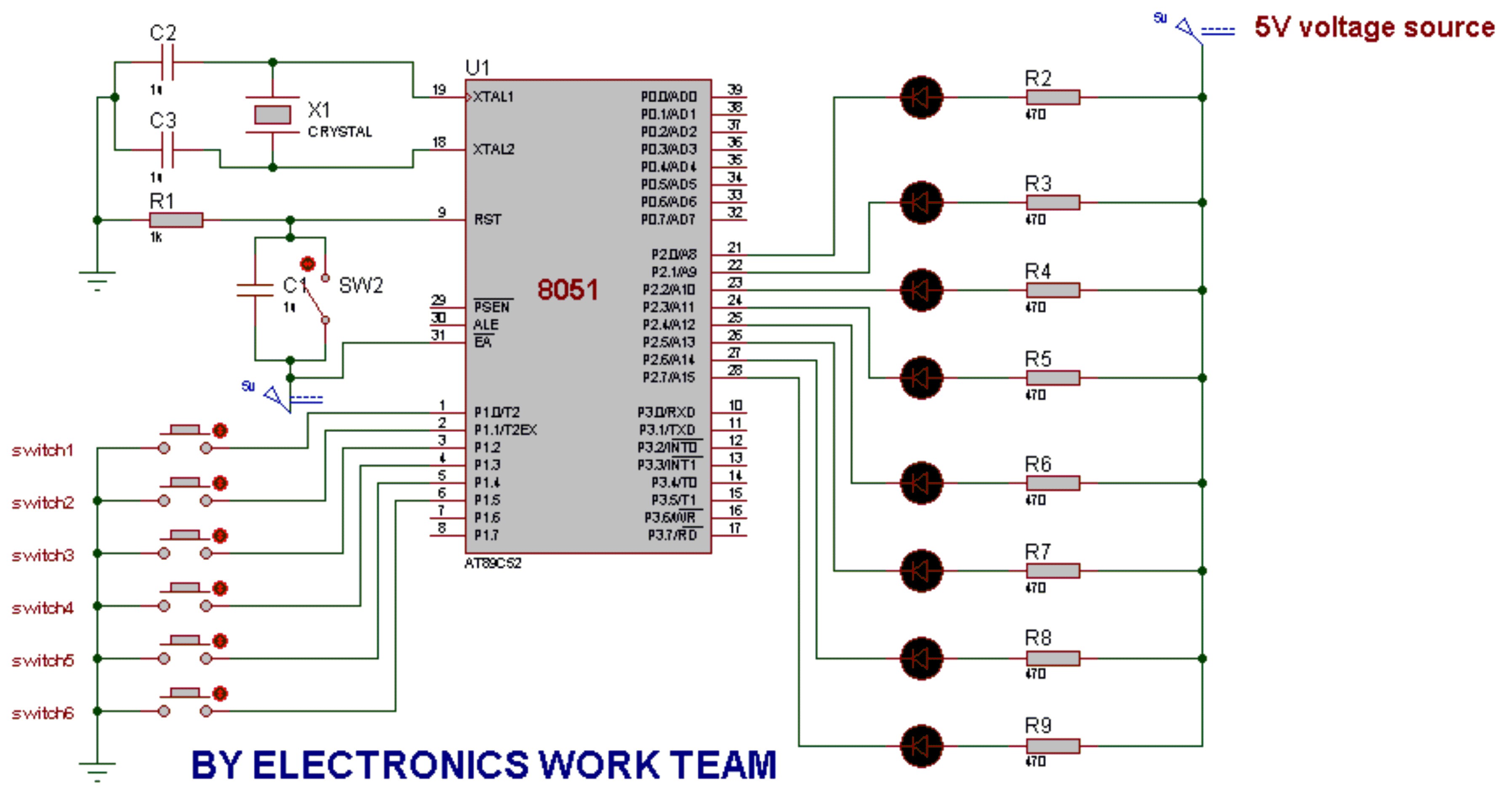
This post discusses the fundamental operation of the 8051 microcontroller using LEDs. The LEDs are connected to the P2 port, while six switches are connected to the P1 port of the 8051. By pressing various switches, the LEDs will...
This robot utilizes two motors to control the rear wheels, while the single front wheel is free to move. It is equipped with four infrared sensors located on the underside to detect black tracking tape. When the sensors identify...
Good preparation. There is one suggestion to use RFM70 or RFM22 for RF communication. The RFM70 and RFM22 are low-power, high-performance RF transceiver modules designed for wireless communication applications. Both modules operate in the 2.4 GHz ISM band, making them...

NOPPP is a straightforward programmer designed for the PIC16C84, PIC16F83, and PIC16F84(A) microcontrollers. It connects to the parallel port of a PC. Plans for this device were published in a magazine. The NOPPP programmer is an essential tool for developers working...
A circuit was discovered in a computer, and there is uncertainty regarding its origin and functionality. The main inquiry is whether this circuit can effectively dim 220V LED bulbs. The circuit in question likely utilizes a phase control method for...
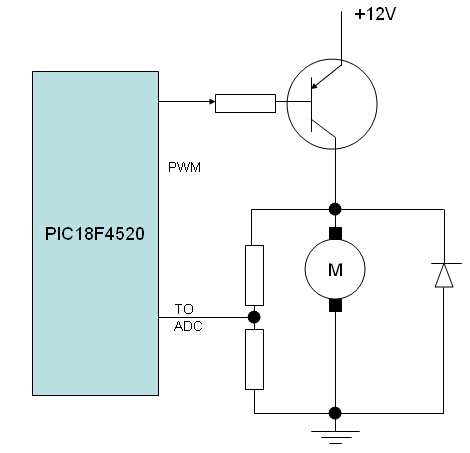
A speed closed-loop control system for a DC motor utilizes back EMF sensing. To implement this, a DC motor is operated in one direction, substituting the LED with the motor and omitting the current limit resistor. It is important...
Warning: include(partials/cookie-banner.php): Failed to open stream: Permission denied in /var/www/html/nextgr/view-circuit.php on line 713
Warning: include(): Failed opening 'partials/cookie-banner.php' for inclusion (include_path='.:/usr/share/php') in /var/www/html/nextgr/view-circuit.php on line 713