
Current negative feedback voltage divider biasing circuit diagram
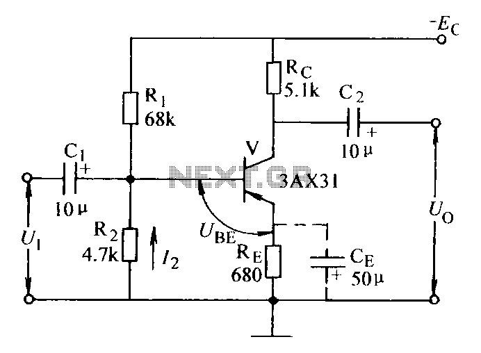
The current negative feedback voltage divider biased circuit is a configuration commonly used in electronic amplifiers to stabilize the operating point and improve linearity. This circuit typically consists of an amplifier, a voltage divider network, and feedback components that work together to maintain consistent performance despite variations in temperature or supply voltage.
In this setup, the voltage divider is formed by two resistors connected in series across the power supply. The junction of these resistors provides a stable reference voltage that is fed back to the input of the amplifier. This feedback mechanism reduces the gain of the amplifier, allowing for better control over the output signal and minimizing distortion.
The feedback loop is critical in ensuring that the amplifier operates within its linear region. The negative feedback effectively reduces the overall gain but improves bandwidth and stability, making the circuit less susceptible to fluctuations. Additionally, the choice of resistor values in the voltage divider directly impacts the feedback level and, consequently, the amplifier's performance.
In summary, the current negative feedback voltage divider biased circuit is an essential design in analog electronics, providing enhanced stability and linearity for various applications, including audio amplifiers and signal processing units. Proper selection of components and configuration is vital to achieving the desired performance characteristics.Current negative feedback voltage divider biased circuit diagram:
Related Circuits
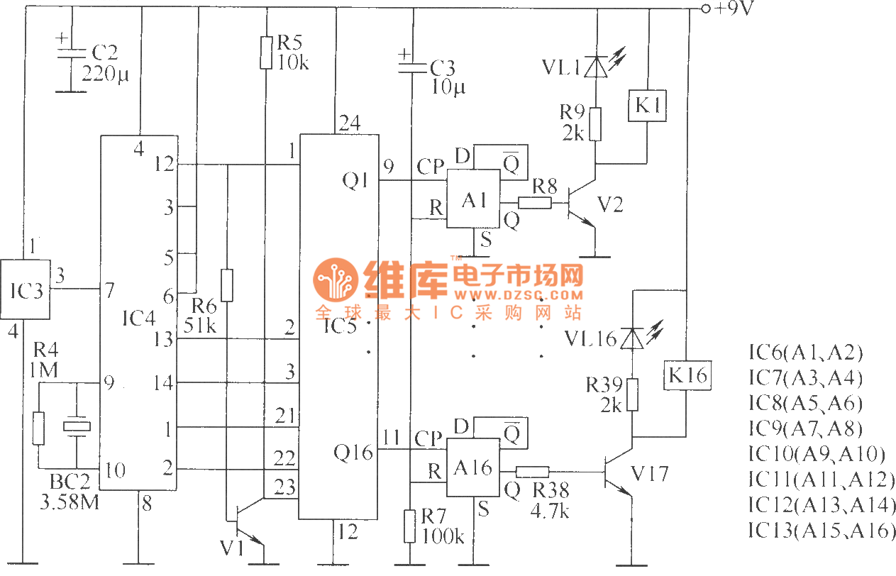
The wireless remote control transmitter circuit consists of control buttons S1 to S16, resistors R1 to R3, a capacitor C1, a regulator diode VS, a crystal oscillator BC1, and DTMF encoder integrated circuits IC1 and IC2. The circuit components...
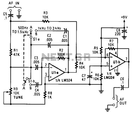
The notch filter can be integrated into nearly any receiver to attenuate a specific frequency by over 30 dB. This filter is particularly useful for diminishing heterodynes and whistles. A notch filter, also known as a band-stop filter, is designed...
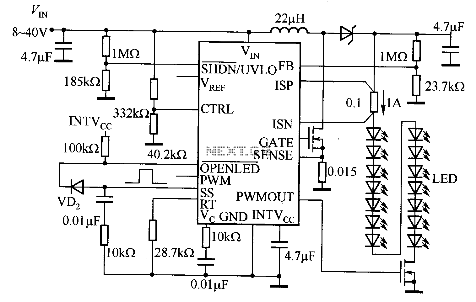
The LT3755 is utilized for high-side current sensing in LED strings, enabling flexible programming and control. It supports a PWM input that allows for a dimming ratio of up to 3000:1, while the CTRL input offers additional analog dimming...
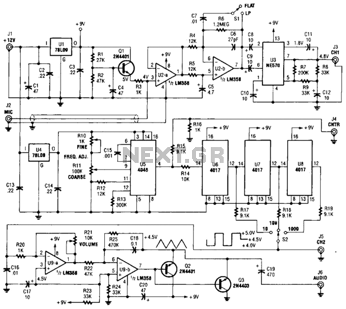
One section of the precision audio frequency generator utilizes an electret microphone element to capture audio from the piano. The captured signal is processed and transmitted to one channel of a dual-trace oscilloscope. The other section of the circuit...
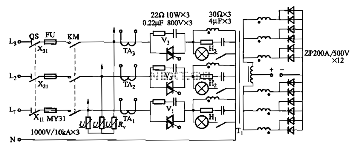
A 1500A-7V phase thyristor power regulator circuit is designed for plating applications. It consists of three major components: the main circuit, the control circuit, and the protection circuit. The control circuit includes a trigger circuit, a synchronous power supply,...
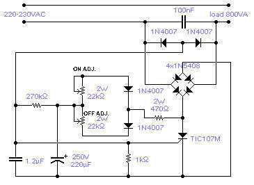
The circuit shown will switch on and off a resistive or inductive load up to 800VA with the possibility to adjust both the on and off period. Switching takes place during the zero crossing of the sine wave. The...
Warning: include(partials/cookie-banner.php): Failed to open stream: Permission denied in /var/www/html/nextgr/view-circuit.php on line 713
Warning: include(): Failed opening 'partials/cookie-banner.php' for inclusion (include_path='.:/usr/share/php') in /var/www/html/nextgr/view-circuit.php on line 713