
Darkroom circuit one time exposure
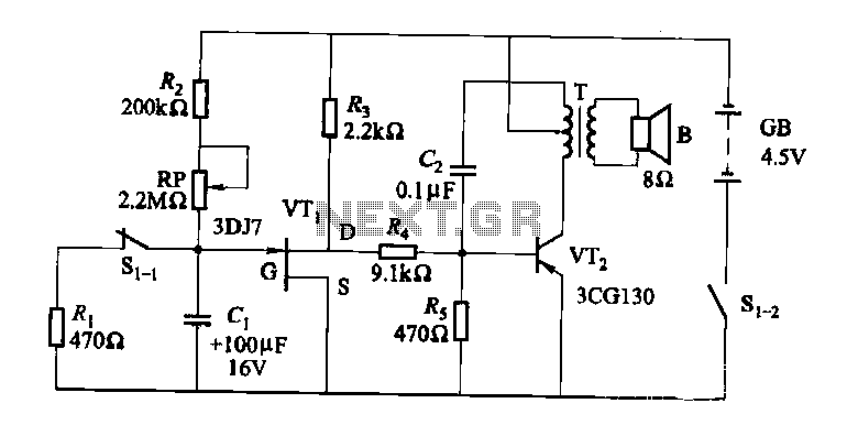
The darkroom circuit for one-time exposure is a practical solution for timing applications in photographic development. It includes several key components that work together to provide a reliable timing mechanism. The circuit utilizes a field-effect transistor (FET), specifically VTi, which plays a crucial role in controlling the current flow and ensuring efficient operation of the timing function.
Resistors and capacitors are strategically included to shape the timing intervals. The potentiometer RP allows for user-adjustable timing, ranging from a minimum of 1 to 1.5 minutes to a maximum of 10 to 15 minutes, depending on the resistance set. This flexibility is essential for accommodating various exposure requirements and ensuring precise control over the development process.
The audio signal generated at the end of the timing cycle is produced through a combination of the transformer T and sound signal segment B, which drives a speaker or horn. This audible alert serves as a notification that the exposure time has elapsed, allowing the user to take necessary actions promptly.
Capacitor Cz is critical in determining the tone of the audio signal, while capacitor Cl governs the overall delay time. These components must be carefully selected based on their capacitance values to ensure that the circuit meets the desired specifications for both timing accuracy and sound quality.
To initiate the exposure process, switch S must be closed, activating the exposure lamp circuit (not depicted in the schematic). Upon completion of the exposure, it is advisable to disconnect the power supply to prevent unnecessary energy consumption and prolong the life of the circuit components.
Overall, this darkroom circuit design provides an efficient and user-friendly solution for managing exposure times in photographic development, ensuring that users receive timely notifications while maintaining energy efficiency.Darkroom circuit one time exposure It audible signal when the developing time is coming. This circuit can be used to put photofinishing big timer, it can also be used for many other occasions. The FET VTi, resistors, capacitors and other components at a given time segment, by the transistor VTz, transformer T and the speaker sound signal segment is B and so on. When the potentiometer resistance RP adjusted to zero, the timer delay of 1 ~ 1.5 min; RP when resistance is adjusted to the maximum, the timer delay is 10 ~ 15min.
Tone audio signal depends on the capacity of the capacitor Cz, and the delay time depends on the capacitance Cl capacity. Closing the switch s, the exposure start (exposure lamp circuit, not shown), the audible signal at the end of the horn.
And this time should be cut off the power supply to avoid wasting energy.
Related Circuits
Features: 1. The operating voltage is low, functioning with a single supply of 2.0V. 2. Power consumption is minimal, with a supply current of 5 µA at 32 kHz and 130 µA at 1 MHz. 3. It has a...
This guide aims to demonstrate the construction of various filter circuits, specifically low pass and high pass filters, along with additional details. The construction of filter circuits is essential in many electronic applications, as they allow for the selective passage...
Do not use the on-board relay to switch mains voltage. The board's layout does not provide adequate isolation between the relay contacts and the low-voltage components. If mains voltage switching is required, mount a suitably rated relay in a...
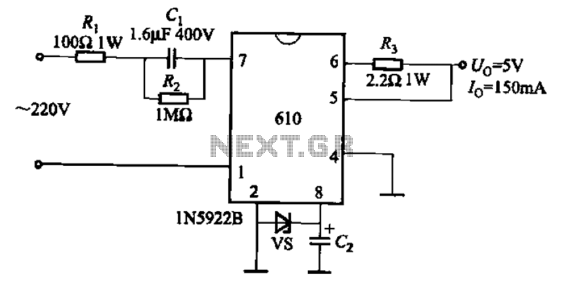
The AX610 Series has a maximum output current of 100 mA and features a scalable output current with an access regulator. The configuration includes two reverse polarity series regulators (2CW106, U: approximately 8.2V) as depicted in Figure (a). Figure...
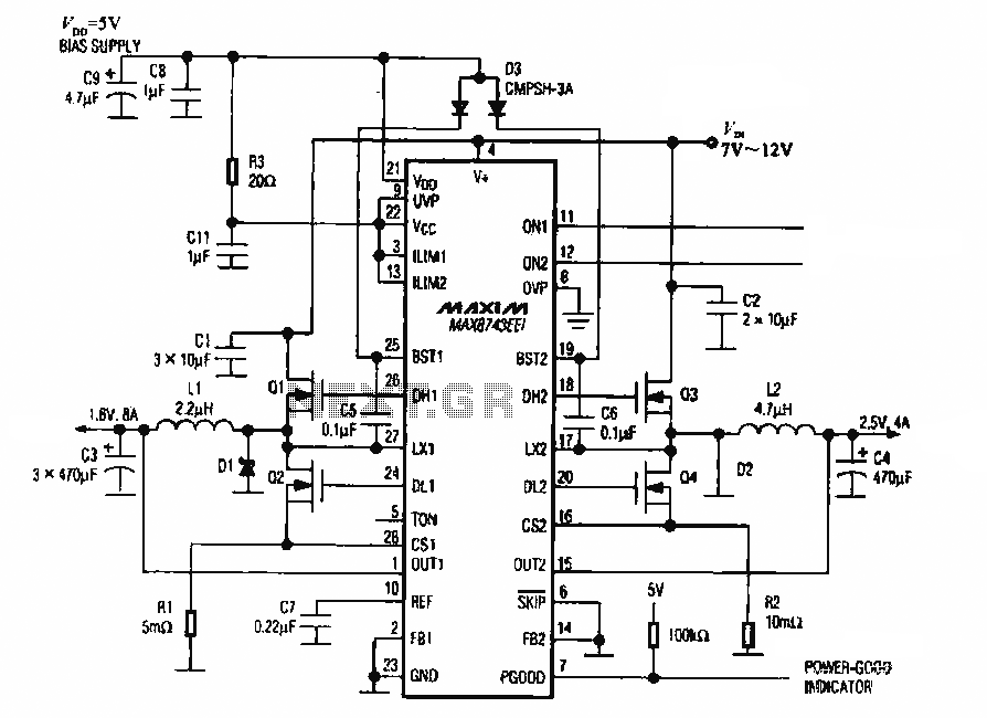
The circuit utilizes the MAX8743 chip for a laptop chipset power supply. It demonstrates the conversion of a 5V power supply into +2.5V and +1.8V outputs. The MAX8743 is a highly integrated power management solution designed specifically for laptop chipsets....

An AC-coupled unity gain voltage follower operating on a single supply is illustrated. The voltage divider network consisting of resistors R1 and R2 provides a DC voltage equal to half the supply voltage to the non-inverting input of the...
Warning: include(partials/cookie-banner.php): Failed to open stream: Permission denied in /var/www/html/nextgr/view-circuit.php on line 713
Warning: include(): Failed opening 'partials/cookie-banner.php' for inclusion (include_path='.:/usr/share/php') in /var/www/html/nextgr/view-circuit.php on line 713