
Darlington amplifier

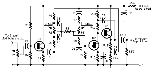
The circuit schematic detailed above represents a sophisticated design aimed at achieving high fidelity and power efficiency in amplification. The twin direct-coupled input amplifier stage, utilizing VT2, is critical for maintaining the stability of the DC operating point through the implementation of local feedback. This feedback mechanism minimizes variations in the output due to changes in temperature or component aging, thereby ensuring consistent performance.
The emitter follower configuration of VT3 serves a dual purpose: it not only stabilizes the voltage levels but also provides a high input impedance while presenting a low output impedance. This characteristic is essential for effective impedance matching with subsequent stages, which is achieved through the impedance transformation process. By ensuring that the output of VT3 is appropriately matched to the input of the push output stage, the circuit can deliver a greater level of push operating current, enhancing overall performance.
VT4, featuring the high-power tube 3DD15, is strategically selected to maximize output power. This component is known for its robust performance in high-demand applications, making it suitable for driving loads that require significant power levels. The integration of VT5 and VT6 into a complementary Darlington configuration further amplifies the output capability, allowing for efficient power delivery while minimizing distortion.
The feedback loop, composed of resistors RF (22 kΩ) and RF (1.2 kΩ), is pivotal in determining the circuit's closed-loop gain. The calculated gain of approximately 25 dB indicates a strong amplification factor, which is crucial for applications where signal integrity and strength are paramount. This configuration allows for precise control over the gain, enabling adjustments based on specific requirements or operational conditions.
Overall, this circuit schematic exemplifies advanced engineering principles in amplifier design, focusing on stability, efficiency, and power output, making it suitable for a variety of high-performance audio and signal processing applications. Circuit schematic shown in Figure 2-3 ov, rlr, VT2 composition twin direct coupled input amplifier stage, the emitter-VT2 VTr base using local feedback to stabilize its DC oper ating point O as emitter follower VT3, impedance transformation used to obtain match drive class, and to provide a greater level push operating current. VT4 push output stage, the use of high-power tube 3DD15, in order to promote greater output power. VTs, VT6 Darlington complementary power output stage. Rf (22kfl) and RF (1.2kfl) composed of the feedback loop and closed-loop gain of the circuit decision.
Av 22/1.2 1. 03, together 25dBo
Related Circuits
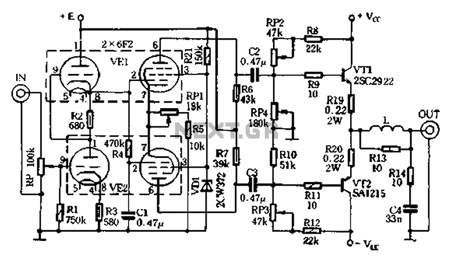
The pre-amplifier stage consists of an inverter made up of two 6F2 pentodes, with pin configurations illustrated in Figure 2.9. The electrical parameters are detailed in Table 2-3. The 6F2 tubes are well-regarded for their intensity and resolving power,...
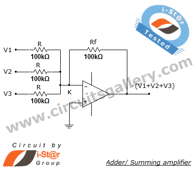
A summing amplifier, also known as an adder, is utilized to combine two or more signal voltages. This voltage adder circuit is straightforward and allows for the addition of multiple signals. It has a wide range of applications in...
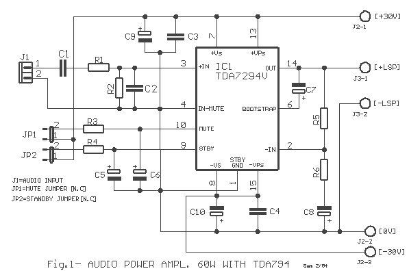
The TDA7294 amplifier module is a monolithic integrated circuit designed for use as an audio class AB amplifier in hi-fi applications. It has a wide voltage range and output current capability, enabling it to supply the highest power into...
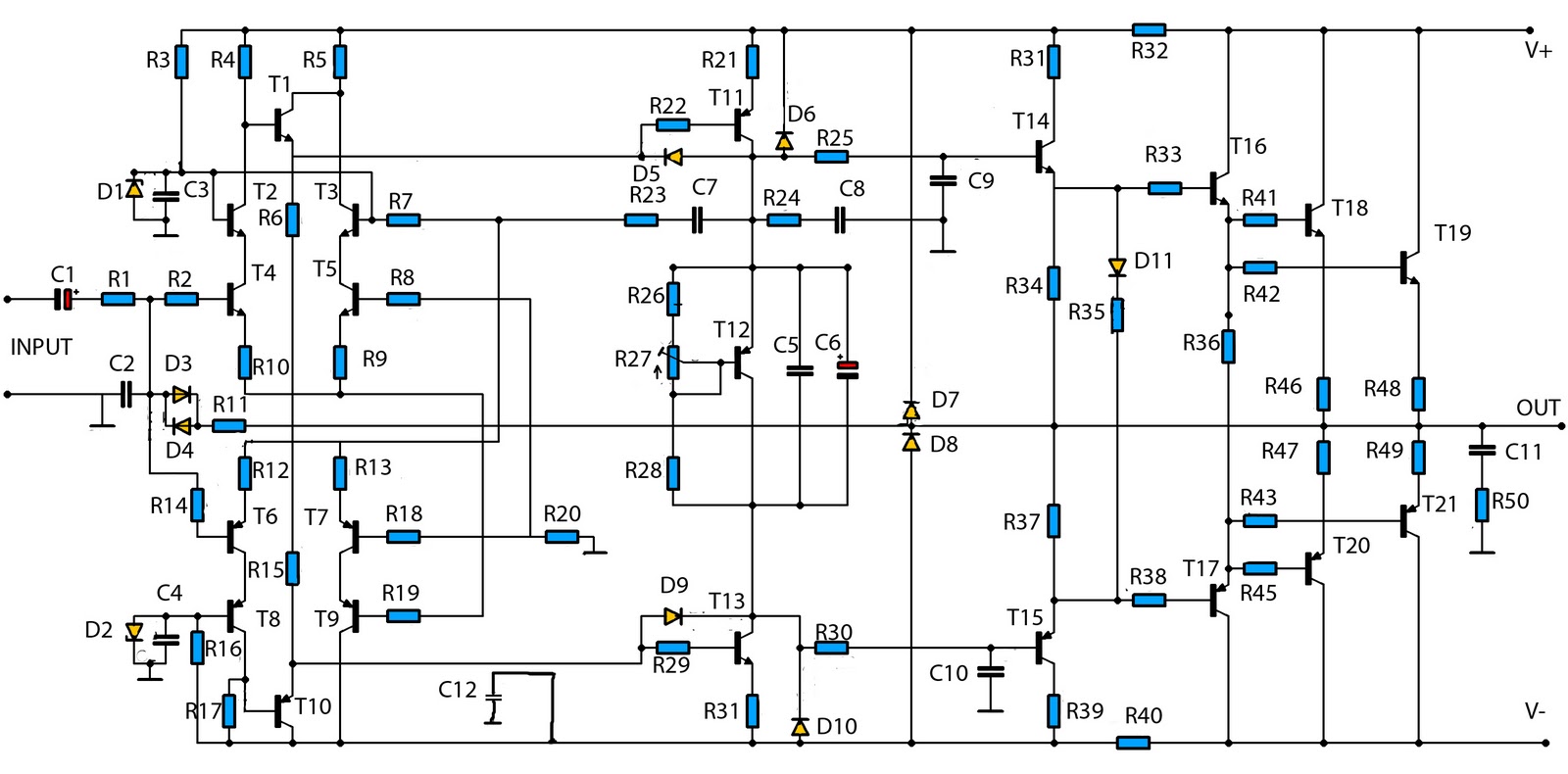
The mono high power amplifier is rated at 1400 W. To create a stereo high power amplifier, which would require a total of 2800 W, the necessary components and PCB must be doubled. The schematic circuit diagram provided is...
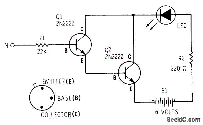
A two-transistor Darlington connection offers a very high input impedance, ensuring that it does not load the logic circuit being monitored. This configuration drives an LED that illuminates when a logic high (1) is present at the input. The two-transistor...
R1 2.2K 1/4W Resistor, R2 27K 1/4W Resistor, R3, R4 2.2K 1/2W Trimmers (Cermet or Carbon), R5 100R 1/4W Resistor, R6 1K 1/4W Resistor, R7, R8 330R 1/4W Resistors, C1 22 µF 25V Electrolytic Capacitor, C2 47pF 63V Polystyrene...