
2800w high power audio amplifier
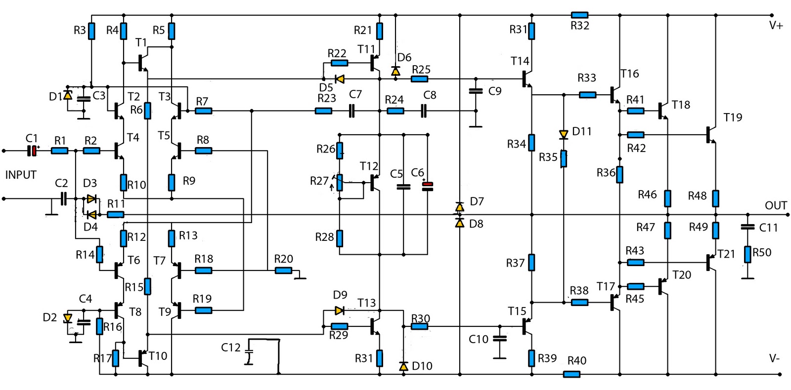
The mono high power amplifier circuit is designed to deliver a maximum output of 1400 W, making it suitable for high-performance audio applications. To achieve stereo sound, the circuit must be duplicated, resulting in a total output capability of 2800 W. This necessitates careful consideration of the power supply, PCB layout, and thermal management to accommodate the increased power demands.
The schematic provided illustrates the basic configuration of the amplifier, which includes gain stages utilizing two JRC4558 operational amplifiers. These op-amps are known for their low noise and high fidelity, which is essential for maintaining audio quality in high power applications. The configuration typically involves using the op-amps in a differential amplifier setup to enhance the signal before it is sent to the output stage.
The amplifier circuit also incorporates various transistors that serve as buffers and drivers. These transistors are critical for managing the current flow and ensuring that the amplifier can drive low-impedance loads without distortion. The choice of transistors will affect the overall performance, including factors such as bandwidth, linearity, and thermal stability.
The booster section of the amplifier, which has not yet been implemented in the current design, is vital for achieving the desired output power levels. This section would typically include additional transistors configured in a push-pull arrangement to drive the output stage effectively. The layout should ensure minimal signal degradation and adequate heat dissipation, as high power levels can generate significant heat.
In summary, the presented high power amplifier circuit is a robust design that, while currently incomplete, lays the foundation for a high-performance audio system. Future enhancements, particularly in the booster stage, will be necessary to realize the full potential of the amplifier in stereo applications.Mono high power amplifier is actually a powerful 1400 W, but if this hihgh power amplifier circuit is doubled and you want to create stereo, high power amplifier the necessary components and pcb requires two-fold. So if the stereo high power amplifier 2 X 1400W. Schematic Circuit diagram is still less by looking at the circuit that was so below, t he finished circuit has been added with a gains using JRC4558 IC by the two and the picture ic where it can be seen below. For circuit buffers, drivers, and booster use multiple transistors and other components (can be seen listed component).
And high power amplifier project that is so below is just part of the buffer and driver while the booster has not been made. For additional transistors in the booster or high power amplifier end scheme can be found Booster output power amplifier.
🔗 External reference
Related Circuits
This single-chip circuit adjusts its audio gain according to the ambient noise picked up by the microphone. When operating in a quiet environment, the audio output is quiet, while a noisy environment results in a louder audio output. Audio...
This amplifier is suitable for various applications that demand high power, low noise, minimal distortion, and superior sound quality. Examples include subwoofer amplifiers, front-of-house (FOH) stage amplifiers, and individual channels of high-powered surround sound amplifiers. For a detailed explanation...
The 13TL amplifier utilizes discrete components and features a complex circuit structure. In contrast, the BTL amplifier circuit structure is simpler and generally performs well with fewer discrete components. Some integrated amplifiers, which are produced on a single integrated...
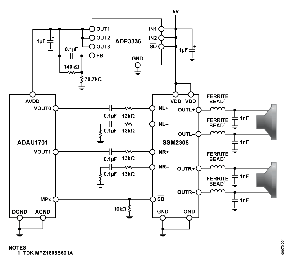
The SSM2306 is a fully integrated, high-efficiency, Class-D stereo audio amplifier designed to maximize performance for portable applications. The application circuit requires minimal external components and operates from a single supply voltage ranging from 2.5 V to 5.0 V....
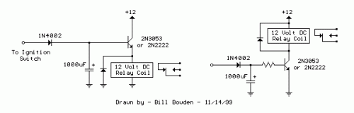
The two circuits demonstrate the operation of opening a relay contact shortly after the ignition or light switch is turned off. The capacitor becomes charged, and the relay remains closed until the voltage at the diode anode reaches 12...
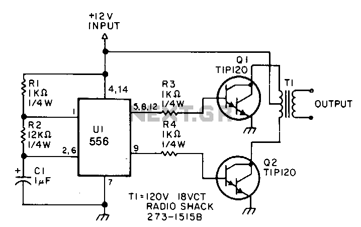
This low-power inverter utilizes only nine components to convert 10 to 16 VDC into a 60 Hz, 115 V square-wave output suitable for operating AC equipment with a maximum power of 25 W. The initial section of the 556...