
DC-10Khz frequency-voltage converter

The described converter operates by utilizing a comparator to detect zero crossings in the input frequency waveform. When the waveform crosses zero, the comparator triggers a response that releases a defined quantity of charge into the summing junction of an operational amplifier (op-amp). This mechanism ensures that the output voltage of the op-amp reflects the input frequency accurately. The feedback resistor plays a crucial role in shaping the output signal, as it determines the gain of the op-amp and thus influences the amplitude of the voltage pulses generated.
The integration of the capacitor (Cint) across the resistor (Rint) is essential for converting the pulsed output of the op-amp into a stable DC voltage. The capacitor averages the rapid voltage fluctuations caused by the pulsed output, smoothing them out to provide a continuous voltage level that corresponds linearly to the input frequency. This averaging process allows for more straightforward measurement and control in applications where a stable DC voltage is required, despite the inherent variability in the input frequency waveform.
Overall, the combination of the comparator, op-amp, feedback resistor, and capacitor forms a robust frequency-to-voltage converter, capable of translating varying frequency signals into a proportional DC voltage output. This configuration is widely applicable in various electronic systems, particularly in frequency measurement and control applications.The converter generates an output voltage which is linearly proportional to the input frequency waveform. Each zero crossing at the comparator"s input causes a precise amount of change to be dispensed into the op amp"s summing junction.
This charge in turn flows through the feedback resistor generating voltage pulses at the output of the op amp Capacitor (Cint) across Rint averages these pulses into a dc voltage which is linearly proportional to the input frequency.
Related Circuits
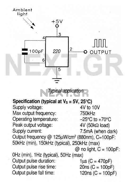
A large area photodiode and current-to-frequency converter integrated into a clear plastic 8-pin DIL package. The output generates a pulse train whose frequency is directly proportional to the light intensity. It is CMOS compatible (a 3.3kΩ pulldown resistor is...
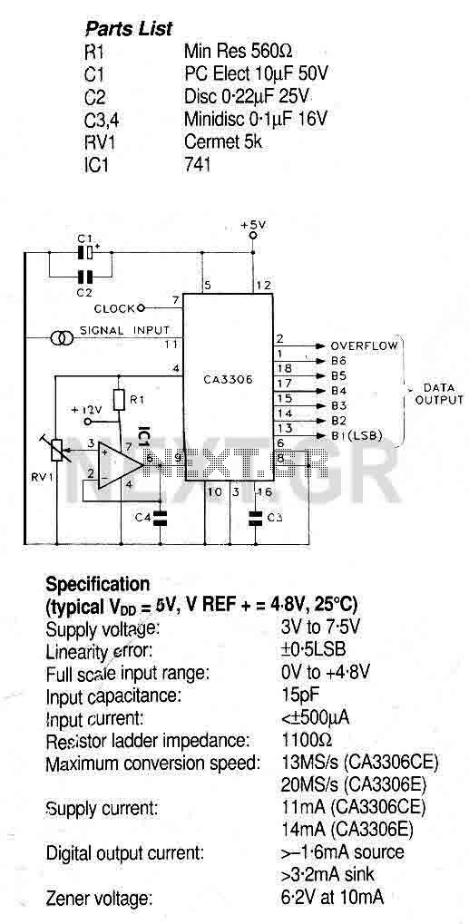
This circuit utilizes the CA3306, a family of CMOS parallel (flash) analog-to-digital converters designed for low power and high-speed applications. The CA3306CE operates at sampling rates of up to 10 million samples per second, while the CA3306E can achieve...
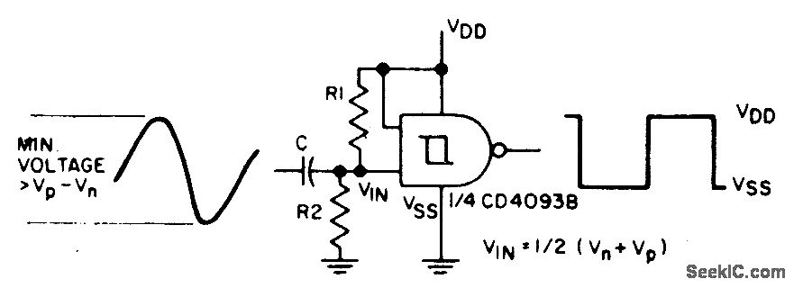
The sine input is AC coupled by capacitor C. Resistors R1 and R2 bias the input midway between Vn and Vp, the input threshold voltages, to provide a square wave at the output. The circuit described utilizes an AC coupling...
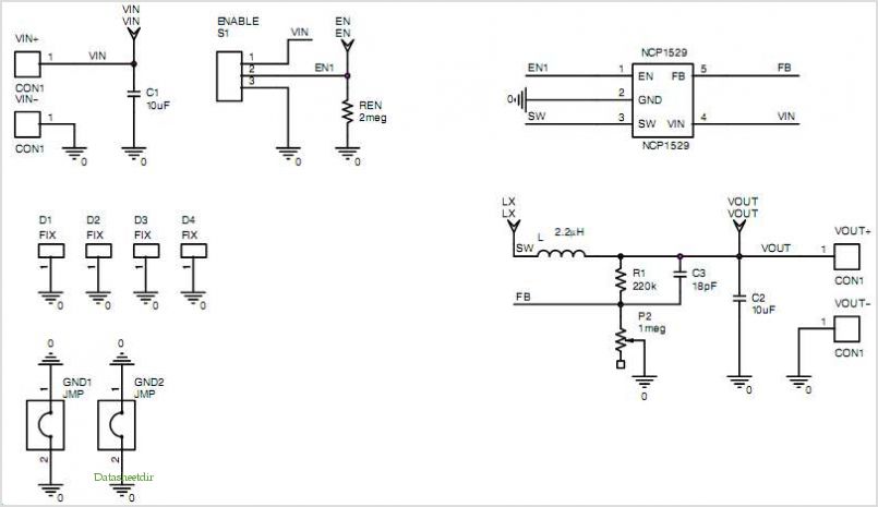
The LinkSwitch-XT LNK363DN-based flyback power supply generates a single isolated DC output voltage from an input voltage range of 90 VAC to 264 VAC. The power supply delivers an output of 5 V at 550 mA (2.75 W) in...
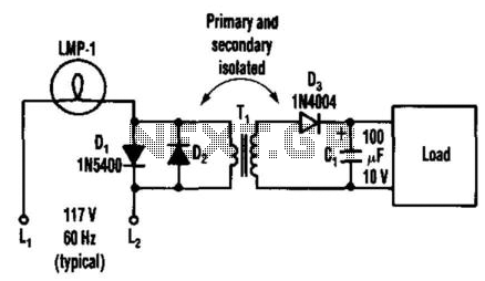
By connecting two back-to-back diodes in series with an AC power circuit, a voltage of approximately 1.4 Vpp can be achieved. This voltage is beneficial for energizing the primary coil of a small transformer. The voltage induced in the...
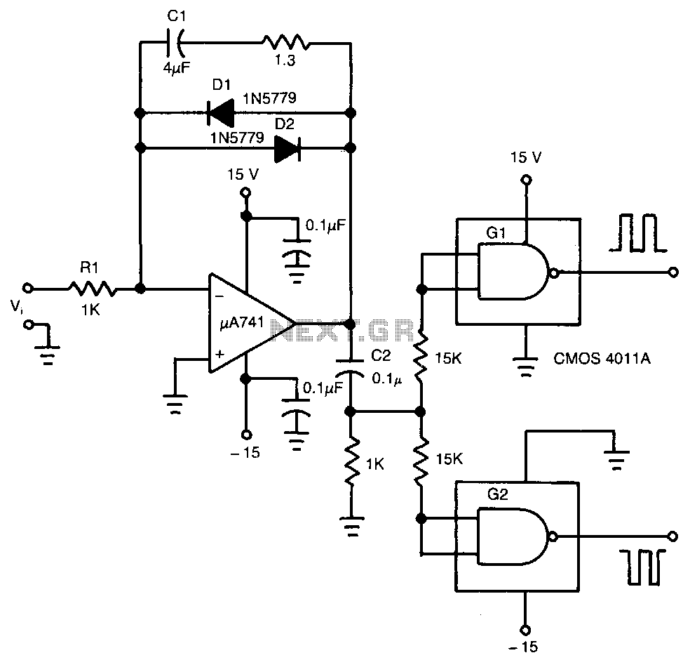
The input voltage, V1, causes capacitor C1 to charge, producing a ramp voltage at the output of the 741 operational amplifier. Diodes D1 and D2 are four-layer devices. When the voltage across C1 reaches the breakover voltage of either...