
Voltage-to-frequency-converter

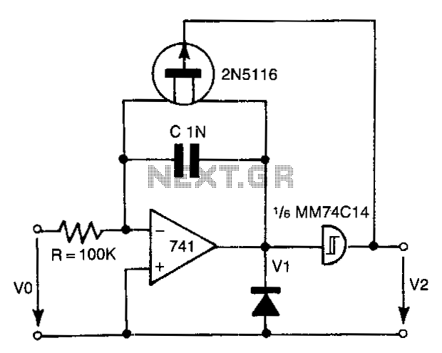
The described circuit utilizes a 741 operational amplifier configured to generate a ramp voltage from an input voltage, V1, through the charging of capacitor C1. The operational amplifier's output will rise steadily until the voltage across C1 reaches the breakover voltage of either diode D1 or D2, which are configured as four-layer devices. Upon reaching this threshold, the diodes will enter conduction, allowing C1 to discharge rapidly. This action results in a sharp drop in the output voltage of the op-amp, effectively generating a narrow pulse.
The coupling mechanism for the discharge pulses is selectively managed through the gates G1 and G2. Positive discharge pulses, resulting from a positive input voltage V1, are routed through gate G1, while negative discharge pulses are directed through gate G2. This configuration allows for the isolation of positive and negative signals, enhancing the circuit's functionality in applications requiring precise signal control.
The circuit's performance is influenced by the forward breakover current characteristics of diodes D1 and D2, establishing a minimum input voltage threshold below which the circuit will not operate effectively. The resistor R1 plays a critical role in defining this threshold; as its resistance value increases, the minimum input voltage also increases, which in turn reduces the dynamic range of the circuit. Specifically, with R1 set to 1 kΩ, the minimum input voltage is observed to be between 10 mV and 50 mV. This characteristic creates an input dead zone, which is advantageous in applications where it is essential for the input signal V1 to surpass a certain level before triggering an output response, thereby preventing false triggering from low-level noise or fluctuations in the input signal.The input voltage, V1, causes C1 to charge and produce a ramp voltage at the output of the 741 op amp. Diodes D1 and D2 are four-layer devices. When the voltage across C1 reaches the breakover voltage of either diode, the diode conducts to discharge C1 rapidly and the op amp output goes abruptly to zero.
This rapid discharge action applies a narrow pulse to G1 and G2. Positive discharge pulses produced by a positive V1 are coupled to the output only through G1, while negative pulses are coupled only through G2. Because of the forward breakover current of diodes D1 and D2, the circuit won"t operate below a minimum input voltage. An increase of R1 increases this minimum voltage and reduces the circuit"s dynamic range. The minimum input voltage with R1 at 1 Kn is in the range of 10 to 50 m V. This input dead zone, when input signal V1 is near zero is desirable in applications that require a signal to exceed a certain level before an output is generated.
Related Circuits
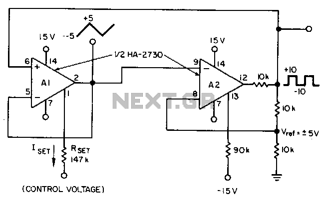
This circuit utilizes a programmable operational amplifier, specifically the HA2730, which is a two-amplifier monolithic chip featuring independent programming ports for each amplifier. The parameters of the amplifiers, including the slew rate, vary linearly based on a set current....
This circuit can accept positive, negative, or differential control voltages. The output frequency is zero when the control voltage is zero. The 741 operational amplifier forms a current source controlled by the voltage Ec to charge the timing capacitor...
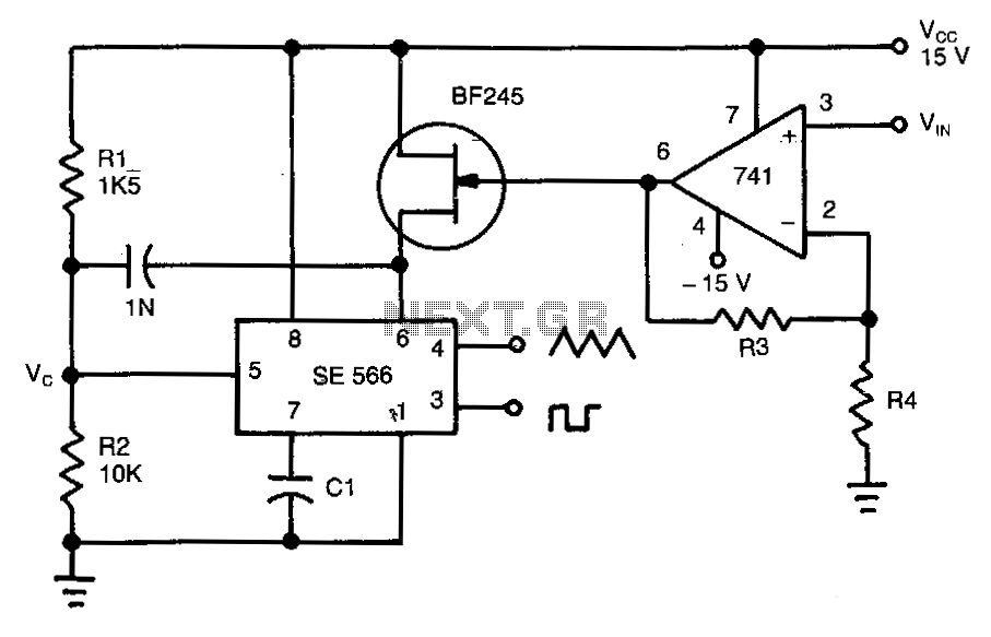
The 741 operational amplifier integrator signal is input into the Schmitt trigger of an inverter. When the signal reaches the positive-going threshold voltage, the inverter's output switches to zero. This output directly controls the FET switch. With a gate...
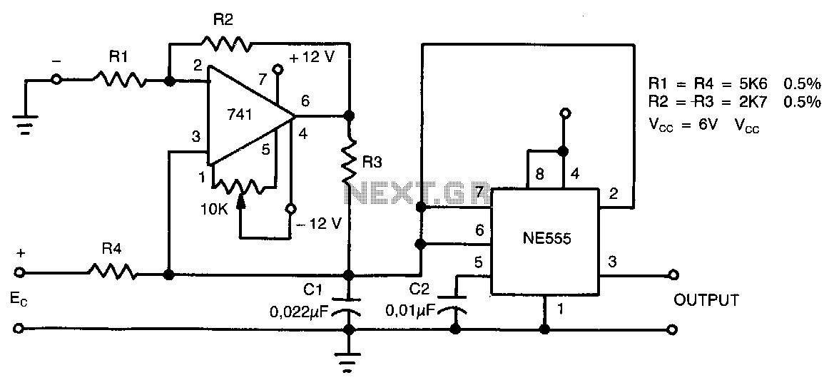
This circuit operates based on the frequency variation of the function generator in relation to the input voltage (ViN). The frequency is influenced by the capacitance and resistor connected to pin 6, with the resistor being substituted by a...
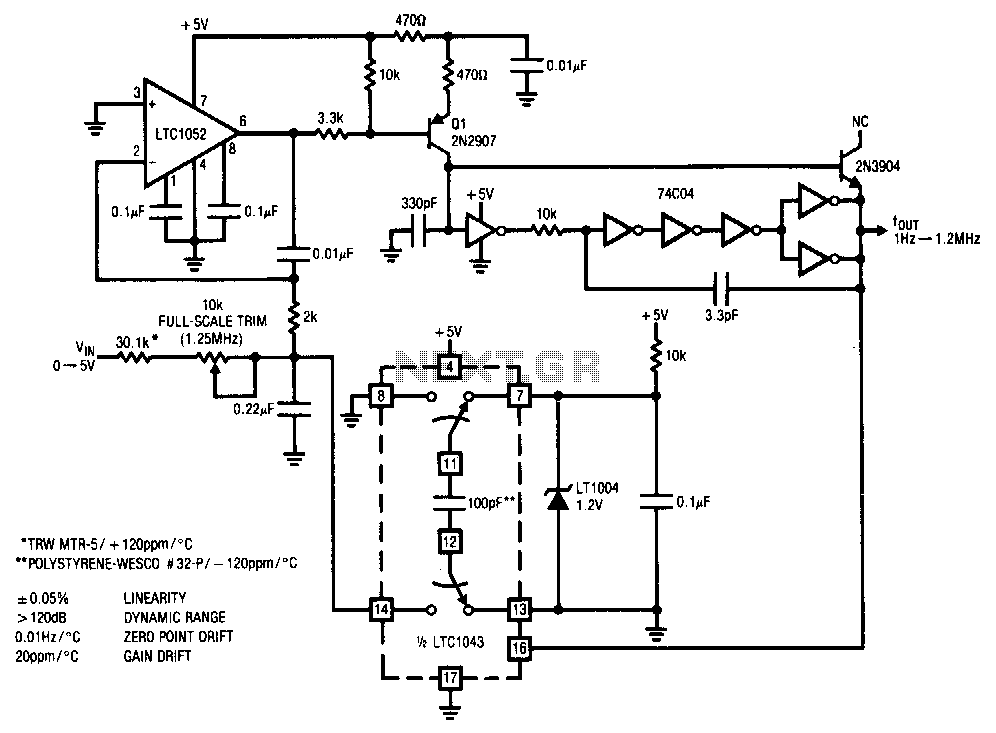
This stabilized voltage-to-frequency converter operates within a range of 1 Hz to 1.25 MHz, featuring a linearity of 0.05% and a typical temperature coefficient of 20 ppm/°C. The circuit is powered by a single 5-V supply. It employs a...
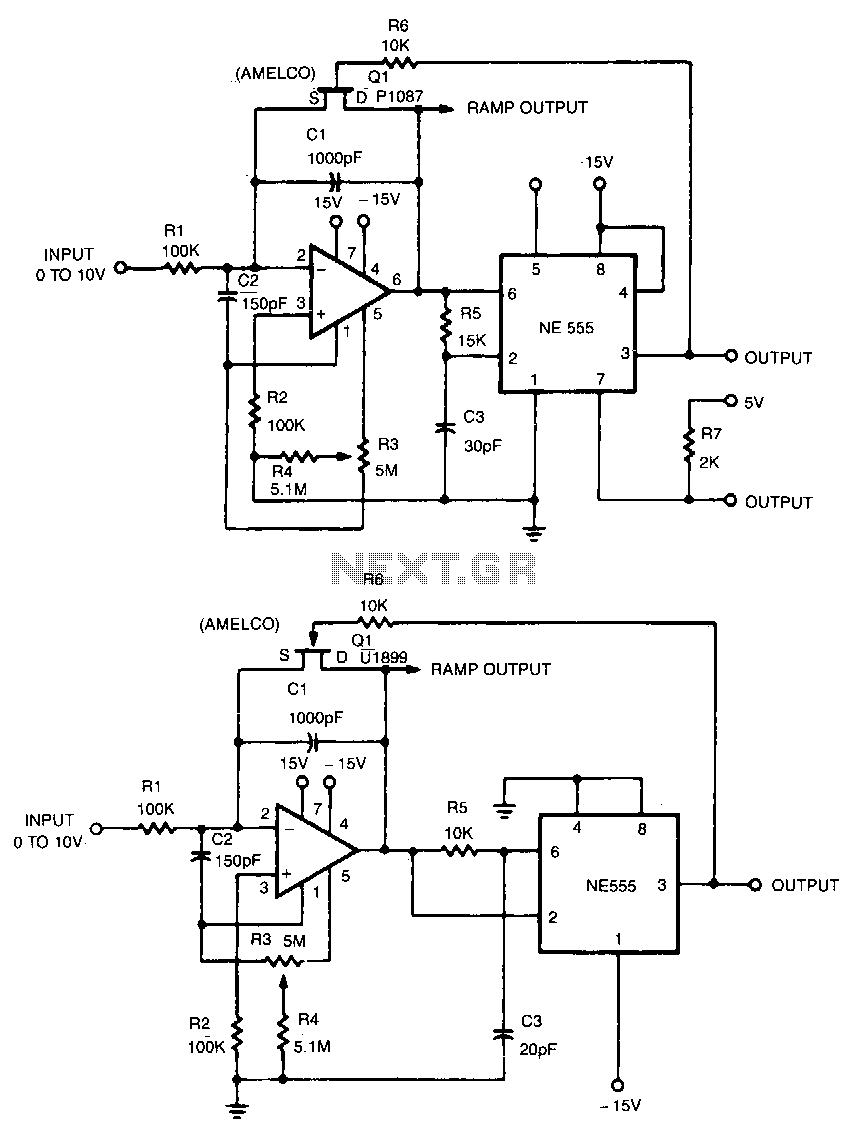
This linear voltage-to-frequency converter achieves good linearity over the range of 0 to -10 V. Its mirror image provides the same linearity over the range of 0 to +10 V; however, it is not compatible with DTL or TTL. The...