
Deeply embedded design

The design of the H-bridge driver circuit is critical for applications requiring precise motor control, such as robotics and automation systems. The six 10 Amp H-bridge drivers are configured to manage the direction and speed of DC motors efficiently. By employing a microprocessor or CPLD for control logic, the design allows for programmable features such as acceleration profiles, dynamic braking, and fault detection, enhancing the overall performance and reliability of the system.
The integration of timing circuits within the control logic is essential for minimizing EMI, which can adversely affect nearby electronic devices. The use of a Schmitt trigger inverter for the rising edge ensures a clean transition, reducing the risk of false triggering due to noise. The fast discharge capability of the open collector inverter on the falling edge contributes to rapid turn-off times, minimizing the duration of high current spikes that can lead to EMI.
The choice of timing components, such as the capacitors and resistors, directly influences the delay characteristics of the circuit. The values selected (10KΩ with 0.1µF and 10Ω with 3.9µF) provide a balance between responsiveness and stability, allowing for fine-tuning of the delays to optimize performance. The design must also consider thermal management, as the high-current operation of the H-bridge drivers generates heat, which must be dissipated effectively to prevent component failure.
In conclusion, the proposed design revision not only addresses the immediate concerns of current spikes and EMI but also enhances the overall functionality and adaptability of the H-bridge driver circuit. By leveraging modern microprocessor or CPLD technology, the design can evolve to meet future requirements while maintaining robust performance in demanding applications.The following is an account of such an undertaking. Recently I was involved in a design review for a cost reduction project, where an older design was getting an update. The new design was a merging of two different designs, including someupdated parts and some existing controls.
The design includes six 10Amp H-bridge drivers and the associated control logic. Some of the early testing had shown some rather large current spikes and also some higher than desirable amounts of electromagnetic interference (EMI). A consultant who had been helping out on a similar design, mostly on EMI concerns, had suggested a few timing changes to the circuitry.
As the talks continued, two different schemes involving changes to the timing were discussed. At this point, I had jumped in and suggested that we pull out all the control circuitry and replace it with a small microprocessor or a CPLD, allowing us some freedom to make changes in the timing schemes. My manager had referred to my suggestion as "a small joke", but I assured him I was serious. A couple of days later I met with my manager and we talked a little more about the idea of handling the bridge control logic inside of a small microprocessor.
After we are able to agree that it would in fact be possible (and also a good idea to do so), we quickly defined the desired level of control and the range of the different delays that we would need to consider. Great, we have a plan and a direction. Before we jump into the work, let`s take a moment and analyze the current circuit to determine present functionality and the actual delay times in order to better understand our starting point.
The big picture view on the circuit is actually quite simple. Changes in the `Direction` line require proper sequencing of the current source and the bridge drivers. On a change in direction, the presently selected drivers (opposite side, top and bottom MOSFETs) are disabled along with the programmable current source.
Then a delay occurs before enabling the opposite set of MOSFETs, along with another delay prior to re-enabling the current source. It is the sequence of these actions and the time delays that will have effects on the operation and resulting EMI characteristics of our six H-bridges.
In the above schematic there are two different delay circuits (two copies using 10K and 0. 1uF, plus one using 10 and 3. 9uF). The direction control circuits each use two different inverters (an open collector type - SN7406 and a Schmitt trigger type - 74HTC14). Each of these inverters are use to control a different edge of the transitions, the Schmitt trigger controls the rising edge (enable), by applying a charging current through a series resistor into a timing capacitor (0.
1uF) to cause a fixed delay, while the open collector inverter controls the falling edge (disable), by using a high current dump of the charge on the capacitor to effect a near zero delay turn off. The combination of the two inverter types is actually a clever approach. The Schmitt trigger device drives both high and low at ~4ma, while the Open Collector device provides no drive in high, but can sink ~40ma during the low state, providing controlled rise time and fast fall time.
The second delay circuit is used to control the programmable current source by temporarily disabling the current source during the direction changes. This stage uses a single Open Collecto 🔗 External reference
Related Circuits
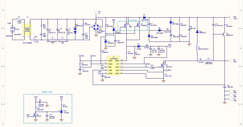
This reference design converts 90V AC to 135V AC input and drives seven or eight series-connected LEDs with an average current ranging from 300 to 600 mA. The LM3445 operates at a nominal switching frequency of 225 kHz. This...
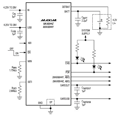
The MAX8844 lithium-ion charger integrated circuit (IC) from Maxim Semiconductors facilitates the design of a simple and efficient charger circuit for a single-cell lithium-ion battery. This charger integrates a current-sense circuit, a MOSFET pass element, thermal-regulation circuitry, and eliminates...
The drop-down category menus above may help you find what you are looking for. Be sure to also look under the Bodo's Power by Topic sub-categories. They include topics similar to our general categories. If the above suggestions were...
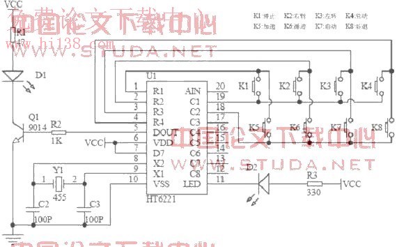
An infrared remote control car utilizes the AT89S51 microcontroller as the core controller. The system operates DC motors via L298 drivers, enabling manual control, autopilot, and tracking functions. The software is modular and developed using the C programming language....

The phase and neutral wires from the power source have already been connected to electrical appliances such as fans and light points. According to the UPS connection diagram, an additional phase wire should be connected to those appliances where...
Voltage inverter circuit design electronic project using few electronic components The voltage inverter circuit is a fundamental electronic project that converts direct current (DC) to alternating current (AC). This circuit is particularly useful in applications where AC voltage is required...