
Demo comparator
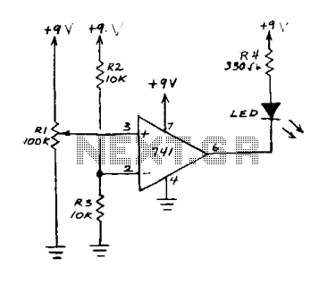
The described circuit utilizes an op-amp in a comparator configuration. In this setup, the op-amp compares the voltage at its non-inverting input (connected to R1) with the reference voltage established at the junction of resistors R2 and R3. The output of the op-amp will switch states based on this comparison.
Resistor R1 is responsible for setting the input voltage level. When this voltage is lower than the reference voltage, the output of the op-amp will go high, activating the LED. The LED serves as an indicator, providing visual feedback regarding the input voltage relative to the reference voltage.
The reference voltage is determined by the resistor divider formed by R2 and R3. By selecting appropriate values for these resistors, the desired threshold for the input voltage can be established. If the input voltage exceeds the reference voltage, the output of the op-amp will drop to a low state, turning the LED off.
This circuit can be utilized in various applications where voltage level monitoring is required, such as in battery management systems, voltage level indicators, or as part of a more complex control system. Proper selection of the op-amp and passive components is crucial for ensuring the desired performance and stability of the circuit.This circuit is an op amp without a feedback resistor. R2 and R3 junction point sets the reference voltage. When the input voltage set by Rl is below the reference voltage the LED glows. If voltage is above reference, the LED goes off. 🔗 External reference
Related Circuits
Comparing the performance of 1200V silicon carbide (SiC) MOSFETs with 1200V silicon MOSFETs and IGBTs at high frequency is essential to identify the differences in device losses and power-handling capabilities among these technologies. A demonstration platform has been developed...
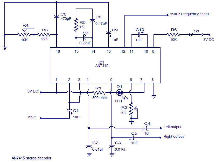
The AN7415 is a monolithic integrated circuit designed for FM stereo demodulation applications. It operates within a voltage range of 1.6 to 7 V DC, making it suitable for handheld FM radios powered by two AA dry cells. This...

The Maya utilized several calendars concurrently, one of which is known as the "long count." This calendar is a continuous record of days starting from a zero date that corresponds to August 13, 3114 BC. According to the Maya...
The TDA3567 is a monolithic integrated decoder designed for the NTSC color television standards. It incorporates all the necessary functions for the demodulation of NTSC signals. Additionally, it features a luminance amplifier and an RGB matrix amplifier. These amplifiers...

A headphone type detection circuit is illustrated in the attached figure. The 2.2k RMIC-BIAS resistor connected to the audio controller provides a low-noise reference voltage (VMIC-REF). When the audio jack is inserted, the VMIC-REF voltage through RMIC-BIAS is applied...
This circuit employs an HgCdTe demodulation device that can be cooled to 77K using liquid nitrogen. It utilizes a constant current bias for the demodulation device, which is connected to the input port. The voltage amplification factor is 200,...