
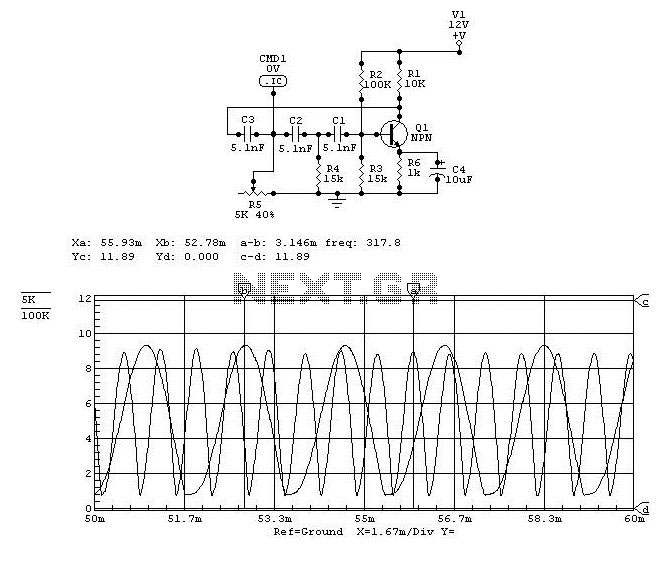
FM Stereo Demodulator by using AN7415

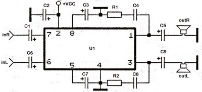
In this circuit, C1 serves as the input coupling capacitor, blocking any DC voltage present in the multiplexed input signal. LED D1 functions as an indicator light, with R1 acting as its current-limiting resistor. Capacitors C4 and C5 are used for DC decoupling in the left and right output channels, while C2 and C3 are noise bypass capacitors for these channels. The potentiometer R2 allows for adjustment of channel separation.
Resistor R5, along with capacitors C7 and C8, creates a low-pass filter network for the internal DC amplifier circuitry, as shown in the block diagram of the AN7415. C10 acts as a filter capacitor for the IC's internal Schmitt trigger amplifier circuitry, and C9 is a ripple filter capacitor for the voltage stabilizer circuit within the AN7415.
Resistor R3, potentiometer R4, and capacitor C6 are responsible for setting the time constant of the internal voltage-controlled oscillator (VCO) circuit, with POT R4 enabling adjustments to the VCO frequency. A 19 kHz frequency check signal is available at pin 12 of the IC. Additionally, switch S1 can be utilized to enable or disable the forced mono function.
The AN7415's design and component arrangement allow for efficient FM stereo demodulation, making it a versatile choice for compact radio applications. The use of low-power components ensures that the circuit remains energy efficient while maintaining high-quality audio output. The inclusion of adjustable elements, such as the potentiometers for channel separation and VCO frequency, provides flexibility in tuning the performance of the demodulator to suit specific requirements. This integrated circuit represents a practical solution for developers seeking reliable FM stereo demodulation in portable devices.AN7415 is a monolithic integrated circuit that can be used in FM stereo demodulation applications. The operating voltage range is 1. 6 to 7Vdc. Two AA dry cells are enough for powering this IC and it makes the AN7415 suitable for handheld FM radio applications. AN7415 has low current consumption (2. 6mA), low distortion, good channel separation and high gain. The IC is available in 16 pin DIL package. The circuit shown below is of a PLL FM stereo demodulator designed based on the AN7415. C1 is the input coupling capacitor which blocks any DC voltage present in the multiplexed input signal. LED D1 is an indicator LED and R1 is its current limiting resistor. C4 and C5 are the DC decoupling capacitors for the left and right output channels. C2 and C3 are the noise bypass capacitors for the left and right output channels. POT R2 can be used for adjusting the channel separation. Resistor R5 and capacitors C7 and C8 forms a low-pass filter network for the internal DC amplifier circuitry (see the block diagram of AN7415).
C10 is a filter capacitor for the IC`s internal Schmitt trigger amplifier circuitry. C9 is a ripple filter capacitor for the voltage stabilizer circuit inside the AN7415. Resistor R3, POT R4 and Capacitor C6 sets the time constant of the internal VCO circuit. Hence POT R4 can be used for adjusting the VCO frequency. A 19KHz frequency check signal is available at the PIN 12 of the IC. Switch S1 can be used for enabling and disabling forced mono function. Be the first of your friends to get free diy electronics projects, circuits diagrams, hacks, mods, gadgets & gizmo automatically each time we publish. Your email address & privacy are safe with us ! 🔗 External reference
Related Circuits
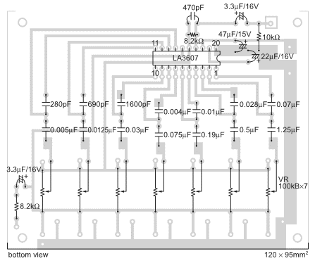
The integrated circuit LA3607 enables the configuration of a 7-band graphic equalizer for a single audio channel by incorporating additional capacitors and variable resistors. The cutoff frequency can be modified using variable resistors. It demonstrates high stability when handling...
The joystick button inputs can be used as general purpose button or switch inputs, and can also be driven by logic level signals or by open collector or open drain logic outputs. If used with a signal direct from...
The TPA2011D1 is a 3.2-W high-efficiency, filter-free Class-D audio power amplifier housed in a 1.21 mm x 1.16 mm wafer chip scale package (WCSP) that requires only three external components. This amplifier features 95% efficiency, an 86-dB power supply...
This series utilizes the TDA2822M integrated circuit (IC) as the primary amplifier. Additionally, alternative ICs such as KA2209, NJM2073, U2822B, and U2823B can be employed alongside the TDA2822M. The output power is limited to a maximum of 4 watts,...
This design circuit is a tachometer circuit based on the LM2907 integrated circuit, which can provide zero-crossing data to a digital system. At each zero crossing of the input signal, the charge pump alters the state of capacitor C1...
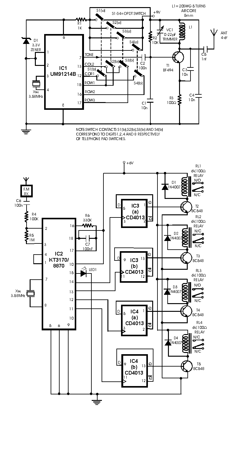
A radio remote control system utilizing DTMF (Dual-Tone Multi-Frequency) technology is presented. This circuit allows for the control of various electrical appliances through radio frequency signals. The described radio remote control system employs DTMF tones, which are generated by a...