
Silicon Carbide MOSFETs Demonstrate Superior High Frequency Performance Under Hard Switched Conditions

The demonstration platform employs a SEPIC converter topology, which is advantageous for its ability to buck or boost voltage while maintaining a non-inverted output. This characteristic is particularly useful in applications where voltage levels need to be adjusted without phase reversal. In this setup, the switch experiences a voltage stress that is double the input voltage, which is critical in assessing the thermal and electrical performance of the tested devices. The SEPIC configuration also allows for flexible control strategies, enabling precise regulation of output current through feedback mechanisms. The integration of a peak current mode control enhances the stability and response of the converter under varying load conditions, making it suitable for rigorous testing of the MOSFETs and IGBTs.
The methodology employed in this testing framework facilitates a direct comparison of the switching losses and thermal performance of the devices under evaluation. The results obtained from this platform can provide valuable insights into the efficiency and operational reliability of SiC MOSFETs compared to traditional silicon-based devices. The use of high-frequency diagnostics, such as the current-viewing resistor and voltage probe, ensures that the measurement accuracy is maintained, allowing for a comprehensive analysis of device performance under realistic operational conditions.Comparing the performance of 1200V silicon carbide (SiC) MOSFETs with 1200V silicon MOSFETs and IGBTs at high frequency is critical to establish the difference in device losses and power-handling capabilities between the technologies. Using a demonstration platform that can be set to emulate a given set of parameters (e. g. , switch voltage, current , frequency and case temperature) that the devices will face at high power under hard-switched conditions, the difference in losses between the device technologies can be characterized by comparing DC input power. Because it is not practical to build separate platforms (retrofitted with SiC devices) for each potential application, (including grid connected solar inverters, power factor correction circuits, motor drives, interruptible power systems, etc.
), it was necessary to design a demonstration platform to overcome this limitation. A transformerless DCDC converter platform with a single ground-referenced switch affords the capability of recirculating the load current back to the input link, eliminating the inherent limitations of a transformer-based platform (prohibitively high losses through proximity and skin effects of the transformer windings at high frequencies). The single-ended primary inductor converter (SEPIC) provides the ability to buck/boost without inverting the output voltage, thus making it an ideal platform to compare relative device performance between SiC MOSFETs and comparably-rated conventional silicon MOSFETs and IGBTs.
The comparison included the best available examples of a 1200V silicon MOSFET (Microsemi APT28M120B2)1, the highest current 1200V silicon MOSFET in a TO-247 package available (its maximum current rating at 100 °C is similar to that of the SiC MOSFET); a 1200V silicon IGBT (Infineon IGW40N120H3)2, a 1200V/40A trench and field-stop device with a forward voltage of 20A, closely matching the SiC MOSFET; and finally, the 1200V SiC MOSFET (Cree`s CMF20120D)3, which has the lowest gate charge with a gate voltage f 20V. All devices were housed in TO-247 plastic packages(see Table 1 for comparative specifications). The SEPIC topology chosen for the demonstration platform is a simple design with a buck/boost characteristic, allowing the converter`s output current to be re-circulated back to the input while the device under test (the switch) is operating at a duty cycle slightly higher than 50%.
SEPIC converter topology is not widely used for high power operation (largely due to high switch stress); however, it is an ideal platform for this demonstration. In this converter, the voltage across the switch is twice the input voltage, and the current through the switch is twice the output current.
Thus, the input DC supply has to provide just half of the desired switch voltage. Furthermore, because the switch is referenced to ground, precise measurements of voltage and current are greatly simplified. As shown in Figure 1, the SEPIC platform schematic consists of a switch (the device under test, or DUT); a diode (D1); a blocking capacitor (C1); output capacitor (C2); and two inductors (L1and L2).
The output current is fed back into the input source (VIN) as shown by the arrows. The controls consist of a simple peak current mode controller, which is fed from a current transformer to sample the drain of the device under test. Input for the current mode controller is supplied from an error amplifier used to regulate the (re-circulated) output current; which in turn is measured by a Hall-effect sensor.
Diagnostics include a high frequency current-viewing resistor to observe the DUT current and a Kelvin-connected voltage probe to measure the DUT voltage. The gate driver is isolated to prevent a ground loop being formed around the currentviewing resistor.
The SEPIC hardware is shown in Figure 2. A lower rack assembly houses the high voltage and logic power supplies along with the SEPIC inductors. The 🔗 External reference
Related Circuits
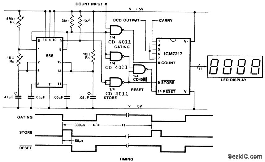
This is an inexpensive frequency counter and tachometer circuit. It utilizes a 556 dual timer to generate the gating, not-store, and not-reset signals for an ICM7217 counter. One timer operates as an astable multivibrator using resistors RA, RB, and...
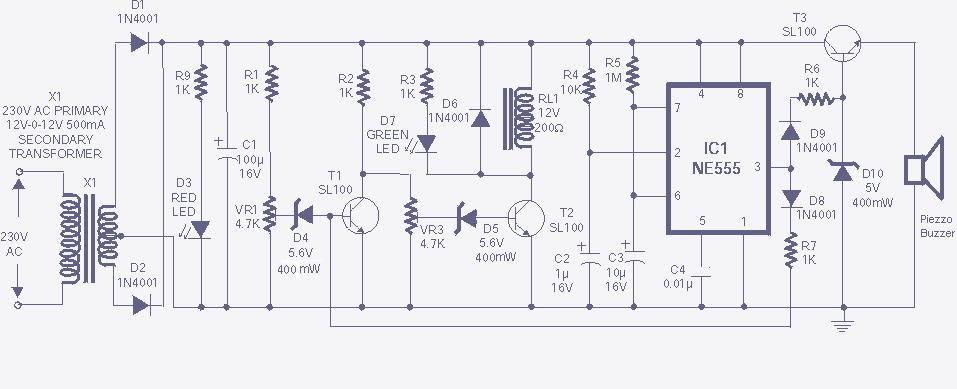
The high and low voltage cut-off with delay and alarm circuit, along with its circuit diagram, is explained in this post. The high and low voltage cut-off circuit is designed to protect electrical devices from damage caused by excessive voltage...
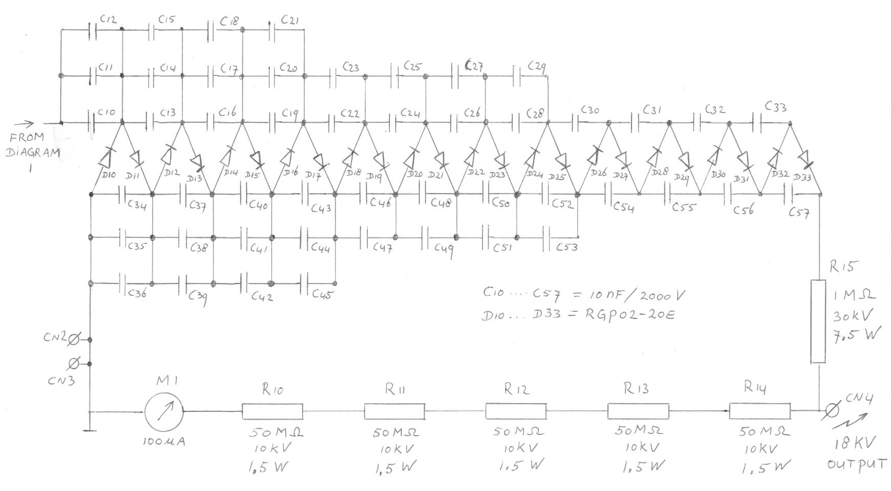
Each subsequent stage adds 1700 volts, resulting in more than 20 kV with 12 stages. However, this voltage can only be achieved when the output of the cascade is unloaded. The described circuit appears to be a high-voltage cascade generator,...
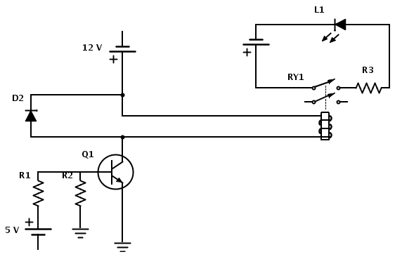
Create a circuit that enables the activation of a relay to control an LED. The relay operates at 12 V, while the available input voltage is 5 V. An NPN transistor will be utilized to switch the power to...
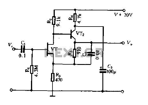
The Field Effect Transistor (FET) exhibits a high input impedance, allowing the construction of high input impedance amplifiers. However, as a FET amplifying device, the distributed capacitance and the Miller effect significantly increase input capacitance at high frequencies. Furthermore,...
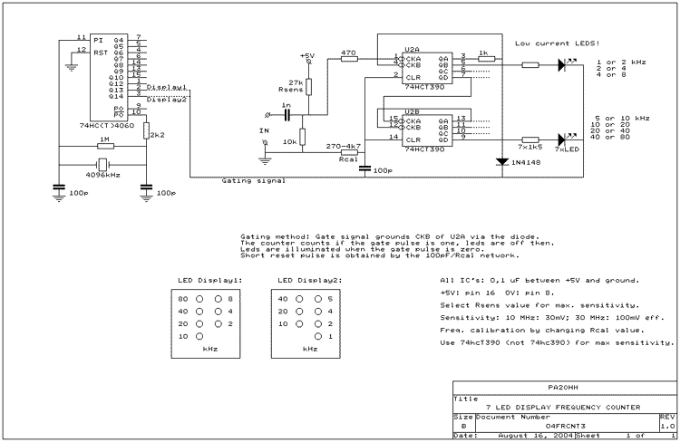
Alternative display methods exist beyond the original 8 LED frequency counter, potentially offering improved readability and a more suitable format for QRP equipment. This document presents examples of binary decimal displays. Typically, the counter omits the MHz position, focusing...