
Demodulating Receiver
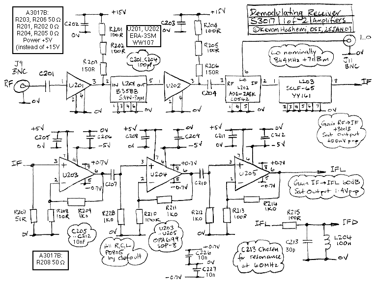
The A3017 Demodulating Receiver is a sophisticated device designed for receiving and demodulating RF signals within a frequency range of 902 to 930 MHz. Its architecture integrates multiple components, including a high-gain amplifier, a downshifter to adjust the frequency of the received signal, and a limiting IF amplifier that ensures signal integrity by eliminating noise. The frequency discriminator and amplitude demodulator work in tandem to extract the desired information from the modulated signal.
The circuit board layout has undergone several iterations to address stability issues, particularly related to oscillations caused by power supply configurations. The modifications implemented, such as the use of copper tape and changes to the power supply voltage, demonstrate a systematic approach to improving performance and stability. The careful consideration of trace width and layer configuration further emphasizes the importance of RF design principles in minimizing signal reflection and maximizing gain.
The thermal noise measurements provide insight into the performance characteristics of the amplifiers, suggesting that even minor variations in component specifications can significantly impact overall system behavior. The design efforts in the A3017B variant illustrate a practical application of engineering principles to achieve a balance between gain and stability, showcasing the iterative nature of electronic circuit design and optimization.
In summary, the A3017 Demodulating Receiver exemplifies advanced RF design techniques, addressing both functional requirements and stability challenges through meticulous engineering and thoughtful component selection. The detailed description of the modifications and performance metrics serves as a valuable resource for engineers seeking to understand or replicate similar designs in RF applications.The Demodulating Receiver (A3017) contains a 902 ’930 MHz 30-dB amplifier, a downshifer, a 60-dB 50-MHz limiting IF amplifier, a frequency discriminator, and an amplitude demodulator. The A301701A circuit board also includes, just for good measure, more copies of the A3016SO SAW Oscillator and the A3008C Spectrometer.
If you can`t understand our terminology (RF, IF, LO, dB, dBm, etc), please consult our Terminology page. [FEB-07] Below you see the A3017A RF Amplifier layout next to its predecessor, the A3016DR RF Amplifier. The former amplifier worked well: 27-dB of stable gain from the RF input to the IF output after the mixer and IF low-pass filter.
Consult the A3016DR manual for measurements of the RF passband. The new, unmodified amplifier, as shown below, oscillates. It`s not the missing capacitors around L201 that stopped oscillation in the previous amplifier. As we describe here, we replaced these capacitors with solder lumps in the previous amplifier, and it was stable. We applied copper tape, cut tracks, changed resistors, and soldered wire links. So far as we can tell, the problem is the loop closed by our +15 V power tracks. In the previous layout, +15 V came up through the ground plane in two separate places for the two amplifier stages.
In this layout, +15 V comes up through the same ground plane penetration. The figure below shows our solution for the A3017A, which is the version we use in the A3018A and A3018B ). Figure: Modification to RF Amplifier Layout for A3017A. We use two rectangles of copper tape to stop oscillations, one 55 mm G— 13 mm the other 10 mm G— 19 mm.
[05-AUG-10] We built three more A3017As using a new batch of ERA-3SM amplifiers. These have slightly different markings. Despite rectangles of copper tape as shown above, the RF Amplifiers of all three units were unstable. At first they passed our tests because they were stable when the input was connected to a 50- © terminator or attenuator, as is the case when we test the Demodulator and when we test reception with an attenuator in series with the antenna cable.
But when the signal is weak at the antenna, and we connect the cable and antenna directly, the RF Amplifier tended to oscillate, especially when we put the lid on the Data Receiver ( A3018B ) that included the A3017A. We measured the thermal noise at point IFL in the circuit for the new A3017A and an older A3017A. The newer A3017A thermal noise was 3 dB larger, which suggests that the newer amplifiers have slightly higher gain, and this higher gain is the source of our intermittent oscillations.
The A3017B uses the modification shown below to stop oscillations in the RF Amplifier. We power U201 and U202 with +5 V instead of +15 V, and use 50 © resistors to deliver the power. This modification reduces the gain of both amplifiers and removes the +15 V power supply loop. The A3017B is stable with and without the lid, with and without the lid screwed in place, and with and without a 50- © terminator on its RF input. The RF to IF gain is around 23 dB, which is 6 dB less than that of the A3017A. The amplifiers provide 20 dB gain with 350- © bias resistors, but only 17 dB with 50- © resistors. We attempt to compensate for the 6 dB loss by increasing the gain of the IF Amplifier, but we doubt these efforts were successful (see below ).
[FEB-07] The printed circuit board traces that connect the amplifiers are 30 mils wide (0. 75 mm). The thickness of the circuit board is 62 mils (1. 6 mm). The circuit board contains four layers of copper traces. The top layer is the one we see in the figure, with the 30-mil traces. The second layer is a continuous plain connected to 0 V, which we call the ground plain. A 30-mil trace 20 mils above a ground plane makes a 50- © transmission line. We want the traces to look like 50- © transmission lines so that they do not reflect RF power (see Terminology ). But we subsequently discovered that the gro 🔗 External reference
Related Circuits
This circuit requires physical connections to be made to the computer's serial port (COM1 or COM2). It is generally considered difficult to cause harm to oneself or the computer through improper connections to this port; however, there is no...
This topic will detail the design of each block of the radio frequency (RF) front-end, taking into account the technical requirements outlined previously. The design aims to meet specific specifications. The RF front-end is a critical component in communication systems,...
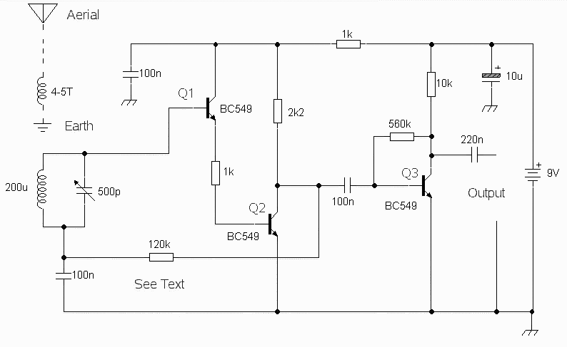
The regenerative circuit is essentially an oscillator circuit equipped with gain control, enabling the user to fine-tune the feedback to a level just below oscillation or, frequently, just above the critical threshold to produce a small oscillation. Typically, a...
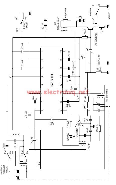
The TDA7088 features a frequency-locked-loop (FLL) system with an Intermediate Frequency (IF) of approximately 70 kHz. This circuit can be powered using a 3-volt battery cell or a regulated power supply. The TDA7088 is a highly integrated FM radio receiver...
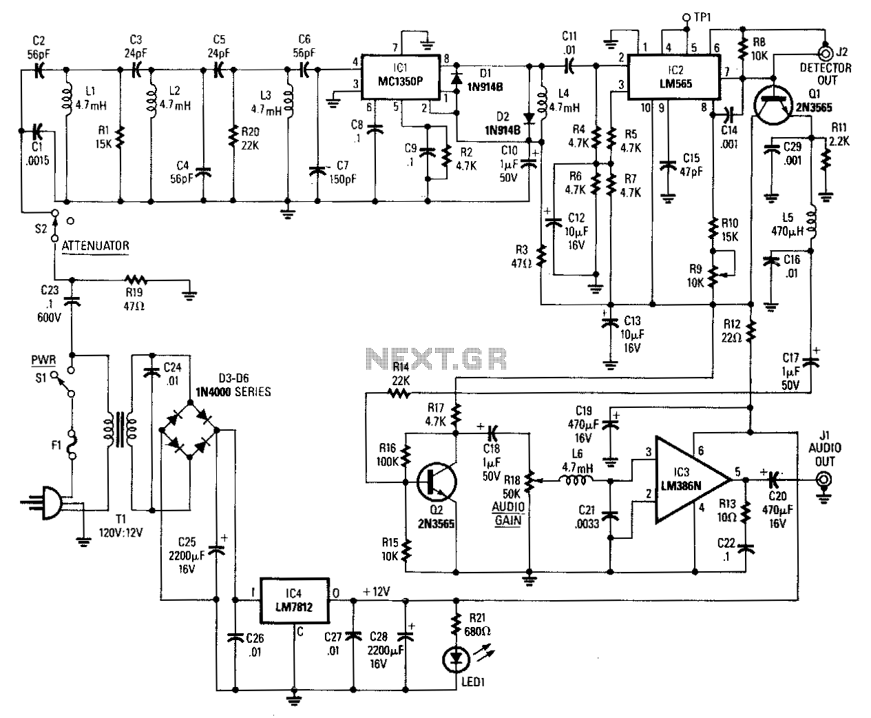
Input signals from the power line are coupled through C23 and R19 to the input filter network. C23 must be rated at 600 volts. Switch 52 is used as an attenuator. Components C2 through C7, L1 through L3, R1,...
The circuit was designed to obtain signals through amplitude modulation, exhibiting good sensitivity and selectivity. Amplitude modulation. The amplitude modulation (AM) circuit is engineered to effectively capture and process radio frequency signals. The design focuses on achieving high sensitivity, allowing...