
Design and making of the stabilized voltage supply of switch

The circuit design incorporates a boost converter topology, which is essential for stepping up the voltage from a lower level to the required output range of 30V to 36V. The boost converter consists of an inductor, switch (typically a MOSFET), diode, and capacitor. When the switch is closed, energy is stored in the inductor, and when the switch opens, the energy is transferred to the output capacitor through the diode, resulting in a higher voltage at the output.
The choice of components is critical for achieving the desired performance metrics. High-efficiency MOSFETs should be selected to minimize conduction losses, and the inductor must be rated for the maximum current to prevent saturation. The output capacitor should have low equivalent series resistance (ESR) to reduce ripple voltage and improve transient response.
The microcontroller chosen for this application must have sufficient processing power to implement the PID control algorithm effectively. The ADC must be capable of accurately measuring the output voltage and current to provide feedback for the control loop. The FPGA will handle the PWM signal generation, which controls the switching frequency and duty cycle of the MOSFET, thus regulating the output voltage.
The design must also incorporate safety features, such as overcurrent protection, which can be implemented using a current sensing resistor and a comparator circuit. If the output current exceeds the threshold, the control circuit can disable the switch, protecting the converter from damage.
Overall, the circuit design aims to achieve high efficiency, stable output voltage, and reliable operation under varying load conditions, making it suitable for a range of applications where precise voltage regulation is required.Under the loading condition of the resistance, output voltage Uo variable range: 30V~36V; Maximum output current LOmax: 2A; When U2 becomes from 15V to 21V, the regulation factor SU of the voltage is less than or equal to 0. 2% Io =2A ; When Io becomes from 0 to 2A, the load regulation S1 is less than or equal to 0. 5% U2 =18V ; The ripple voltage peak-peak value UOPP of the output noise is less than or equal to 1V U2 =18V, Uo =36V, Io =2A ; Efficiency of DC-DC converter is greater than or equal to 85% U2 =18V, Uo =36V, Io =2A ; Have overcurrent protection functions, action current Io th =Unless 2. 5 0. 2A, behind it get rid of on excessive load trouble, power can self-recovery as normal state; Can carry on keyboard presuming and marching adjustment, step-by-step value 1V, measurement and digital display function with output voltage, electric current at the same time to the output voltage; Converter Includes the controlling circuit Can only be supplied power by UIN port, can`t add the accessory power supply.
We need to determine the systematic scheme at first. In requiring, have a little effect on overall scheme, these indexes all only relate to factors such as device choosing, preparation method, etc. , so we focus on three indexes left. First of all, output voltage Uo variable range 30~36V, it is 15- 21V and isolate the secondary of voltage transformer and export, commutate and strain wave rear about 27V the most, is smaller than 30V, obviously needs boost to export within the range of whole voltage.
Certainly, the topic has no rectifying circuit form of restriction, another kind of solution is that voltage doubling is commutated and filtered again first, the final-stage like this can adopt the voltage dropping circuit. Secondly, require the whole efficiency of the converter to be greater than 85%, for low-powered power, this requirement has been already higher, can calculate, under power rating of 72W, 85% of the efficiency, loss of converter can`t exceed 12.
7W, want, meet requirements for this, must use, try hard little devices, whether power or main circuit, or control the measurement circuit, should make it try hard to be simple. The topic still requires the power of the controlling circuit to only commutate the delivery port UIN Draw, can`t add the accessory power supply, this demands to make the accessory power supply by oneself, and accessory power supply efficiency is not too low, so the linear power is not the ideal choice.
From the above-mentioned analysis, we obtain the overall demand: The main circuit needs to use boost topologically, and boost is not big in range, the circuit structure should try hard to be simple, the device quantity tries hard to make the accessory power supply by oneself little, and efficiency, in conformity with the great. Analyze that can also discover, it is required that Input/Output was not isolated, and the input terminus has already isolated the voltage transformer to isolate, so can choose Input/Output and have no topological structure of electric isolated circuit.
We select the basic Boost boost-up circuit scheme finally, the control device chooses and insults 16 one-chip computers of male genital, production of driving signal choose FPCA, system whole the intersection of scheme and picture the following is show. 220V alternating current stepped down, commutated, strained Bode`s more stable direct-current volts, the direct-current volts is strained Bode`s smooth dc output again by Boost circuit boost, the output voltage, electric current are sampled input AD and changed the chip, realize by controller, PID of one-chip computer, voltage regulation and voltage regulation then export the command signal, give FPGA, and go on, reveal, FPGA produces PWM signal by gas switching tube of the driving circuit propulsion power to realize loop-locked feedback control.
Produce the guard signal of the excessive load when 🔗 External reference
Related Circuits
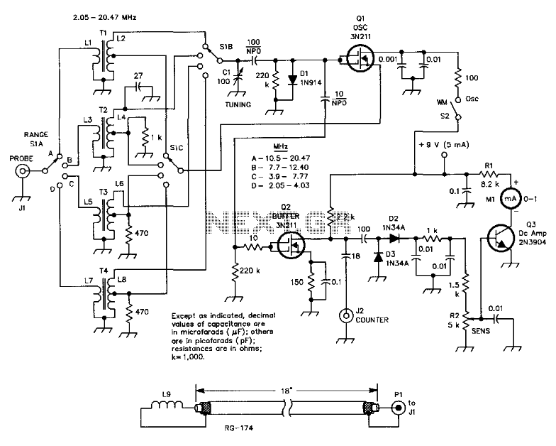
This circuit is designed for checking resonances in tuned circuits, antennas, and similar applications, covering a frequency range of 2 to 20 MHz. Q1 acts as an oscillator that can be tuned across this range using capacitor C1 and...
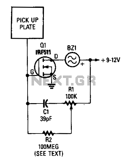
A 3x3-inch piece of circuit board, or a similarly sized metal object, serves as the pick-up sensor connected to the gate of Q1. A 100 MΩ resistor, R2, isolates Q1's gate from R1, ensuring that the input impedance remains...
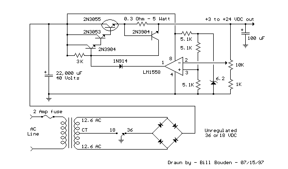
This regulated power supply can be adjusted from 3 to 25 volts and is current limited to 2 amps as shown, but may be increased to 3 amps or more by selecting a smaller current sense resistor (0.3 ohm)....
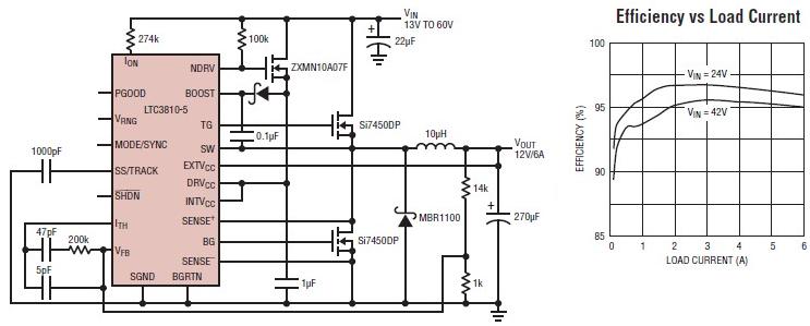
The LTC3810-5 synchronous step-down switching regulator controller allows for the design of a straightforward 12-volt switching power supply electronic project with minimal external components. This controller can directly reduce voltages from up to 60V, making it suitable for telecommunications...
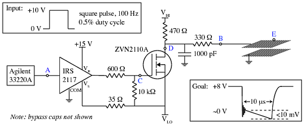
A copper mesh measuring 10 cm x 10 cm is situated in a vacuum chamber and connected to a BNC connector via a 24 cm copper wire. The objective is to rapidly switch the voltage across the mesh (referenced...
Field bus technology and intelligent instrument technology are currently two of the most rapidly evolving technologies in automation and control. In the realm of field bus technology, the CAN bus has established itself as a relatively fast communication standard...