
Digital Clock
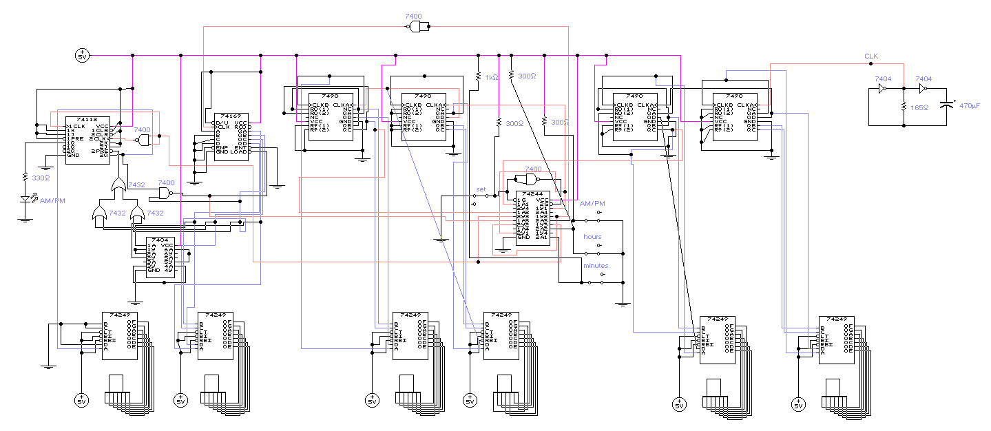
The 7490 decade counter is a critical component in timekeeping applications, providing precise counting capabilities. It utilizes a negative edge-triggered mechanism, ensuring accurate transitions during clock cycles. The connection of pins CLKB and QA is essential for the counter's operation in decade mode, allowing it to count from 0 to 9 effectively. The asynchronous reset functionality provided by inputs R0 and R9 enables immediate control over the counting process, allowing resets to 0 or 9 based on the logic levels of these inputs.
The dual counter configuration, where one counter counts seconds and the other counts minutes, is a common design in digital clocks. The right counter's design, which triggers the left counter upon reaching a count of 9, ensures a seamless transition from seconds to minutes. The connection of outputs QB and QC from the left counter to the reset inputs is a clever design choice, allowing for a controlled reset at the appropriate counting threshold.
The incorporation of JK flip-flops for the hour digit representation and AM/PM indication adds flexibility to the design. The toggling mechanism driven by the clock pulses allows for accurate representation of time in a 12-hour format. The use of NAND gates to manage the LOAD functionality and the connections to the BCD-to-7 segment decoder ensures that the output remains consistent and accurate for display purposes.
The tri-state buffer enhances the design by providing isolation between different stages, preventing unwanted interactions during the setting process. The push-button interface allows for user-friendly adjustments to the clock, enabling easy setting of minutes, hours, and AM/PM indication. Overall, this design represents a robust and efficient approach to digital timekeeping, utilizing well-established electronic components and principles to achieve accurate and reliable performance.The 7490 counter is a negative edge triggered decade counter that counts from 0 to 9. Pins CLKB & QA must be connected for this counter in order that it would operate in the decade mode. The inputs R0(1, 2) & R9(1, 2) are asynchronous reset pins, one of each must be low for counting, if both the R9(1, 2) inputs were high, then the counter will be res et to 9, while if both the R0(1, 2) inputs were high while one of the R9(1, 2) inputs was low, then the counter will be reset to 0. Since the number indicating the minutes or seconds consists of 2 digits, then 2 counters are used, the one on the right counts from 0 to 9, while the one on the left counts from 0 to 5.
For the counter on the right, the bit QD goes from HI (ie: 1) to LO (ie: 0) only in one condition, that is when the count goes from 9 to 0 (ie. from 1001 to 0000 in binary), so, it is used to trigger the counter which is on the left, so whenever the count goes from 9 to 0 at the counter on the right, the counter on the left will be triggered and incremented by 1, till the count becomes 6.
For the counter on the left, the outputs QB & QC are connected to the R0(1, 2) inputs, so when the count becomes 6, the counter will be immediately reset to 0. Hence this stage will count from 00 from 59. Since the output QC for the counter on the left goes from HI to LO only when it is reset from 6 to 0 (ie.
0110 to 0000 in binary), so, it is used to trigger the counter in the next stage. The seconds stage is triggered by a 1 Hz astable multivibrator stage, the minutes stage is triggered by the QC output of the seconds stage (which is labelled "out CLK pulse" in the figure), and the hours stage is triggered by the QC output of the minutes stage. Since the maximum hour is 12, then the first digit is either 0 or 1, therefore only one bit is needed for this digit, hence a dual JK flip flop is used, one JK is for this first digit, and the other flip flop is used for the AM/PM indication.
The J & K inputs are connected together in each JK flip flop, so, the flip flop`s state will be toggled at the next CLK pulse. Consider the NAND gate which is below the 74168 counter, one of its inputs is the Q output of the JK flip flop which is used to indicate the first digit for the hours, and the second input is the QB output of the 74168 counter, the output of the NAND gate is connected to the LOAD input of the 74168 counter, which is an active low input, when activated, the data on the A, B, C, D inputs appear on the QA, QB, QC, QD outputs at the next CLK pulse respectively.
The B, C, D inputs of the 74168 counter are connected to GND, so they are LO, while input A is connected to VCC, so it is HI, so the inputs ABCD are equivalent to 0001 in binary, which is 1 in decimal. When the hours = 12, then the output Q of the JK flip flop which is used to indicate the first digit for the hours is equal to 1, and the QB output of the 74168 counter will also be 1, so the LOAD input will be activated, and at the next CLK pulse 0001 will be loaded on the counter outputs, then the LOAD input will be equal to 1 and therefore de-activated, and so, the 74168 will continue counting starting from the next CLK pulse.
Note that the output of the NAND gate is also connected to the CLK input of the JK flip flop which is used to indicate the first digit for the hours through an inverter, so when the LOAD goes HI, the CLK of this JK flip flop will go LO which will trigger this flip flop & its output Q (which is HI) will be inverted (ie. it will be LO), and so, when the present state of the hours stage is 12, the next stage will be 01. When the 74168 counter goes from 9 to 0, the output of all the OR gates that are below the dual JK flip flop will be LO, since the output of the upper OR gate (which is LO only when outputs of both lower OR gates are LO) is connected to the PRESET input of the JK flip flop which is used to indicate the first digit for the hours, which is an active LO input, when activated, it will make the output of the JK flip flop equal to 1, and therefore, when the present state of the hours stage is 09, the next stage will be 10.
The output of the NAND gate which is below the 74168 counter is connected to the CLK input of the JK flip flop used for AM/PM indication, and therefore, whenever the present state of the hours stage is 12 the Q output of this flip flop will be toggled. Note : for the JK flip-flop indicating the first digit of the hours, only one output is required for the BCD-to-7 segment decoder, and it will be connected to the A input of the decoder, while the other inputs B, C, & D will be grounded (ie.
equal to zero) Since the clock has to be set, so a tri-state buffer is used to separate different stages that are to be set. This tri-state buffer is the the 74244. When 1G is LO, the outputs 1Y1, 1Y2, 1Y3 & 1Y4 follow the inputs 1A1, 1A2, 1A3 & 1A4 respectively, and when 2G is LO, the outputs 2Y1, 2Y2, 2Y3 & 2Y4 follow the inputs 2A1, 2A2, 2A3 & 2A4 respectively.
When 1G is HI, the outputs 1Y1, 1Y2, 1Y3 & 1Y4 are in high-impedance state, similarly when 2G is HI, the outputs 2Y1, 2Y2, 2Y3 & 2Y4 are in high-impedance state. A push button which is normally closed is used to set 1G LO & 2G HI (note the inverter between 1G & 2G), when 1G is LO, the clock is in the counting mode, for example, when the seconds stage count goes from 59 to 00, then the minutes stage count will be incremented by 1, and when the minutes stage count goes from 59 to 00, then the hours stage count will be incremented by 1, and when the hours stage count goes from 12 to 01, then the AM/PM indication will be toggled.
When the push button controlling 1G & 2G is pressed, then 2G is LO & 1G is HI, and the clock is in the set mode, for example if the push button controlling 2A1 (the "set minutes" push button) is pressed, then 2A1 will go from HI to LO, and the minutes stage count will be incremented by 1, also if the push button controlling 2A2 (the "set hours" push button) is pressed, then 2A2 will go from HI to LO, and the hours stage count will be incremented by 1, also if the push button controlling 2A3 (the "set AM/PM" push button) is pressed, then 2A3 will go from HI to LO, and the AM/PM indication will be toggled. 🔗 External reference
Related Circuits
This circuit is designed for precise centigrade temperature measurement. It features a transmitter section that converts the sensor's output voltage, which is proportional to the measured temperature, into frequency. The output frequency bursts are transmitted through the mains supply...
This circuit employs switched emitter followers instead of conventional analog switch CMOS chips, resulting in a more effective reduction of crosstalk between channels. It can manage up to 4 Vms with less than -80 dB crosstalk. The circuit design utilizes...
This project involves using an EasyDriver stepper motor driver and a 1.8-degree per rotation stepper motor to achieve a motor speed of one revolution per minute. The EasyDriver simplifies the operation, requiring a DC voltage of 7-30V connected to...

The circuit described is a crystal oscillation circuit using a CM OS inverting configuration, designed to ensure accurate operation. It employs a BCD counter (IC2) capable of achieving a maximum oscillation frequency of 2 MHz, which is 100 times...

Normally, an analog-to-digital converter (ADC) requires interfacing through a chip to convert analog signals into digital format. This necessitates both hardware and software, resulting in increased complexity and overall cost. The circuit presented here is configured around the ADC...
This is a portable oscilloscope adapter that can be held in a breast pocket. Its operation is only sampling and sending to the host PC. Most of the functions of the oscilloscope are processed by the host PC. Therefore,...
Warning: include(partials/cookie-banner.php): Failed to open stream: Permission denied in /var/www/html/nextgr/view-circuit.php on line 713
Warning: include(): Failed opening 'partials/cookie-banner.php' for inclusion (include_path='.:/usr/share/php') in /var/www/html/nextgr/view-circuit.php on line 713