
Digital Clock
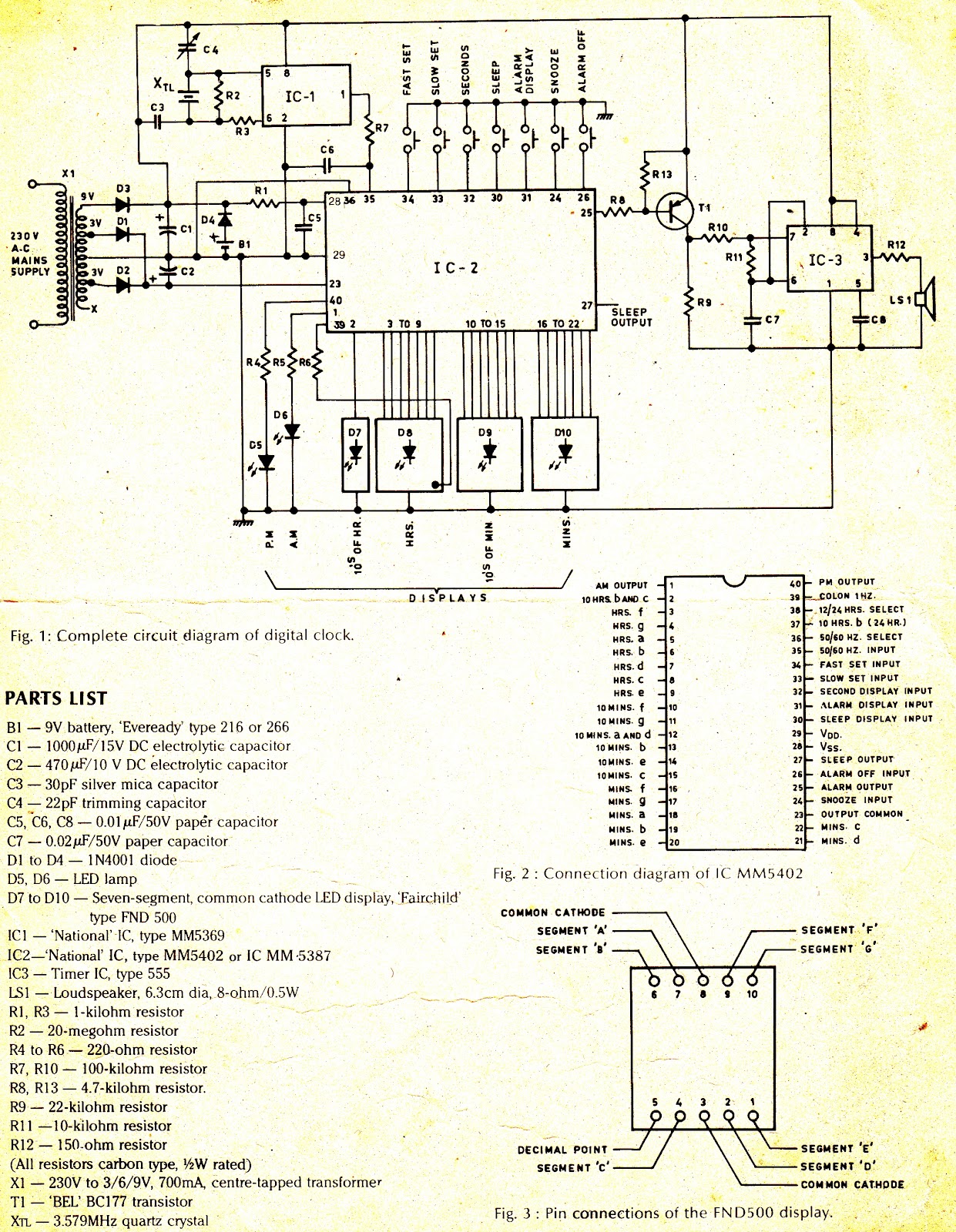
The circuit operates on a well-defined architecture, leveraging the capabilities of the MM5402 clock chip and the MM5369 frequency divider to maintain accurate timekeeping. The design incorporates essential components such as the step-down transformer, diodes, capacitors, and LEDs, which work together to create a functional timekeeping system. The choice of components ensures reliability and ease of assembly, making it suitable for both amateur and professional applications. The inclusion of a battery backup system enhances the robustness of the circuit, ensuring continued operation during power outages, which is critical for time-sensitive applications. Additionally, the use of a relay for sleep timer functionality allows for versatile control over connected devices, enhancing the overall utility of the clock system. The design emphasizes simplicity in user interaction through push-button controls, providing a user-friendly experience while maintaining technical integrity.The complete circuit diagram is shown in Fig. 1. Heart of the system is lC2, National`s MM5402 clock chip. It is an MOS monolithic large scale integrated circuit. It`s pin configuration is shown in Fig. 2. The supply is derived from the mains through a low-voltage stepdown transformerXl. As shown in the diagram, 9-volt DC supply derived by diode D3 and capacitor Cl is fed to the counting circuit of the clock chip at pin 29 through a lk resistor. A bypass capacitor C5 is used at r input of clock chip for protection from high-frequency transients.
The current requirement for the entire clock chip is around 4. 5 mA. . The clock input pin 35 is fed by 60Hz clocked pulses. These are derived by 3. 579 MHz quartz crystal oscillator formed with ICI, Nationals MM5369 chip, which is also ia frequency divider. Its output at pin I is 60Hz square wave For trimming the crystal frequency, a trimmer (C4) is also provided which could be used for improving the accuracy of time.
For display, Fairchild`s FNDSOO seven-segment light emitting diodes (LEDs), D7 to D10, are used. These are common-cathode LEDs. Since the clock chip`s segment output is of the order of lO mA, no interfacing is required. The various LED segments are only to be connected to the respective clock outputs. In all, four LED displays are required, and these can be straightaway soldered on to a separate PCB or breadboard. Supply to the display LED is obtained from the 3V tap of transformer Xl. The pin configuration of FND500 is shown in Fig. 3. The blinking colon is also available in the FND500 display. It is provided at pin 5 of the display, and may be connected through a 220-ohm current limiting resistor to pin 39 of the clock chip.
The a. m. and pm. displays are obtained by using two LED lamps, D5 and D6, and connected to pins I and 40 of clock chip through 220-ohm current limiting resistances. All the U`Eplay functions are obtained by simply connecting push-button switches at various control inputs, and grounding the respective input.
In the prototype a self- assembled seven-reed assembly of switches was used. However, though costlier, the miniature calculator keyboard switches made by O/E/N India Ltd are the best for this purpose. Alarm output is available at pin 25 of the clock chip. Since this output is quite low, a current driver is used. This driver is formed by the transistor Tl and a few supporting components, as shown. Fora gentle alarm sound, tone is generated by lC3, which is an Indian timer IC 555. The tone can be varied by changing the value of capacitor C7. An 8 ”ohm, 0. 5- watt speaker of 6. 3 cm dia should produce sufficient sound to be heard across the room. _ The sleep output at pin 27 of the clock chip is similarly amplified and used to drive a relay which can control any audio or electrical equipment.
The function of sleep timer is to switch off a radio set, tape recorder, TV etc after a preset time, within the maximum duration of 59 minutes. Since the clock chip as well as the crystal oscillator-cum- divider IC operate on 9V supply (actual operating range : 7 to ll volt), a battery back ”up system can be used to keep the clock running during mains failure.
There will be no display of time while the clock is running on this back-up system, but on the resumption of power through AC mains the clock will automatically display the correct time. lf due to any reason supply to the clock chip is cut off, all the digits will flash at lHz to indicate that time displayed is incorrect.
🔗 External reference
Related Circuits
This page describes a cheap and simple yet flexible HDMI to parallel 3.3V interface. This allows connecting most LCD frames to the BeagleBoard without any further interface required. It is used with some 7-inch 800x480 displays running Angstrom Linux...
The schematic diagram depicted in Figure 1 is designed to synthesize a sinusoidal waveform with a frequency range of 0.01 Hz to 1 MHz. A clock signal is supplied to the input of the binary counter IC1, with a...

The 3130 CMOS operational amplifier provides the necessary high input impedance for a pH probe at a low cost. The output of the probe varies from a positive generated DC voltage for low pH values to 0 V for...
This document describes the function of a digital stopwatch that counts from 0 to 99 seconds. The stopwatch utilizes four integrated circuits from National Semiconductor, although alternative components could achieve similar results. The circuit diagram is presented in an...
This is the new and improved nixie clock utilizing one of the smallest nixie tubes available, the Russian IN-17 nixies. The clock circuit is based on revisions of the version 1 nixie clock that were utilized in the Single...
This post discusses the interfacing and operation of Analog-to-Digital Converters (ADCs). An ADC is a device that converts the analog signals from transducers into digital signals, enabling computers to process the data. ADCs are essential for obtaining meaningful results...