
Digital Entry Lock Circuit
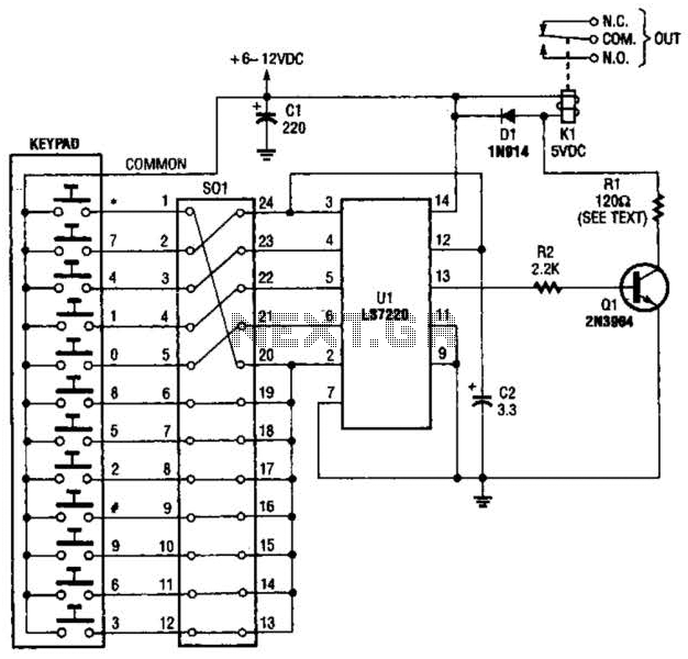
The LS7220 keyless-lock IC operates as a secure access control mechanism, utilizing a keypad interface for user interaction. The design features a 24-pin socket configuration, where each of the 12 keys from the keypad connects to dedicated pins on the IC, enabling precise detection of key presses. The common connection to the positive supply rail ensures that pressing any key sends a high voltage signal to its corresponding wire, facilitating the identification of the pressed key.
Programming the access code involves configuring jumpers on a 24-pin header, which allows for flexibility in setting unique codes based on user requirements. The sequence of the four-digit code is critical; the system is designed to recognize the specific order of key presses. Upon successful entry of the correct code, the IC activates an output signal at pin 13, which is crucial for controlling external devices through the relay mechanism.
The transistor Q1 acts as a switch that is controlled by the output from the IC. When the output at pin 13 goes high, current flows through resistor R2 into the base of Q1, turning it on. This action pulls the collector of Q1 to ground, allowing current to flow through relay K1, which then closes its normally open contacts. This operation can be utilized to control various devices such as electronic locks, alarms, or other automated systems.
Capacitor C2 plays a vital role in timing the output signal duration, ensuring that there is sufficient time for the user to enter the complete access code. The choice of capacitance directly influences the timing; hence, an increase in capacitance will proportionally extend the time window for key entry, thereby enhancing usability. This design consideration is critical in applications where user error in key entry sequence could lead to system failure. Overall, the LS7220 keyless-lock IC provides a robust solution for secure access control, combining user-friendly operation with reliable electronic performance. A block pinout diagram of the LS7220 keyless-lock IC is shown. The keypad must provide each key with a contact to a common connection. In this case, the common connection goes to the positive supply rail so that when a key is pressed, a positive voltage is passed through to the wire associated with that key. Each of the 12 keys are brought out to separate wires, and each wire is connected to a different pin of a 24-pin socket (SOI).
To activate (unlock) the circuit, a preprogrammed four-digit access code must be entered in the proper sequence. The four-digit access code must be entered in the proper sequence. The four-digit access is programmed into the circuit by connecting jumpers between terminals of a 24-pin plug-in header. When the correct access code is entered (in the proper sequence), positive voltages appear at pins 3, 4, 5, and 6 of Ul.
That causes IJ1 to output a positive voltage at pin 13, which is fed through resistor R2 to the base of Ql, causing it to conduct. With Ql conducting, its collector is pulled to ground potential, energizing relay Kl. The normally open relay contacts close, switching on any external device. Capacitor C2 controls the total time that the output of Ul at pin .13 is positive after the release of the first key.
With a value of 3.3 for C2, active time after release of the first key is about two seconds, assuming a 6-V supply or four seconds with a 12-V supply. Therefore, if you push the subsequent keys too slowly, the relay might not close at all! To increase the time allotted for code entry, you will have to increase the capacitance of C2. 🔗 External reference
Related Circuits
A small (2 to 3 meters) neon electronic transformer circuit diagram is provided below. The described circuit diagram is intended for use with neon lighting systems, specifically those requiring a transformer to operate efficiently within a range of 2 to...
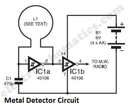
The metal detector circuit presented here exemplifies simplicity while demonstrating effective functionality. It utilizes a single 40106 hex Schmitt inverter IC, a capacitor, a search coil, and batteries. A connection from IC1b pin 4 must be made to a...
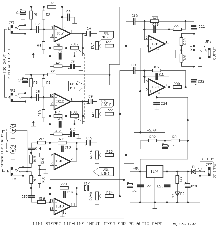
Most cards of sound in computer are deprived stereo input for microphone; on the contrary, they have stereo input for high level (Line). The circuit uses the input Line of the sound card in order to connect two mono...
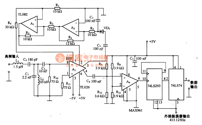
This is an FSK modulation circuit composed of the 74LS74. The FSK modulation circuit does not include a phase-locked loop (PLL) or a high-Q bandpass filter, eliminating the need for tuning adjustments in the high-frequency modulation circuit. The two...
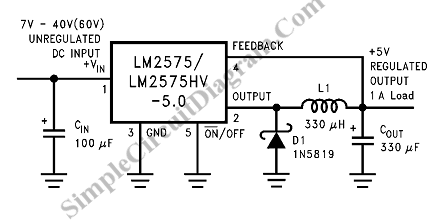
Switching Regulator for High Power Efficiency. When it is necessary to convert a high voltage to a significantly lower voltage, a switching regulator is the optimal choice. A switching regulator is an essential component in modern power management systems, particularly...
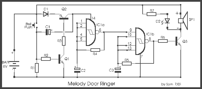
In all the houses exist the bells in the door. All want, they have the possibility of being possible to change the intensity, the tone of sound. With this circuit we have this possibility. With the materials round the...
Warning: include(partials/cookie-banner.php): Failed to open stream: Permission denied in /var/www/html/nextgr/view-circuit.php on line 713
Warning: include(): Failed opening 'partials/cookie-banner.php' for inclusion (include_path='.:/usr/share/php') in /var/www/html/nextgr/view-circuit.php on line 713