
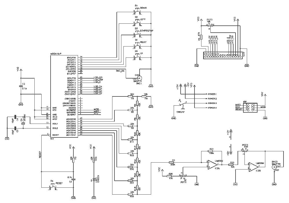
Digital Function Generator (MEGA16-P)
Buttons LEFT and RIGHT were reversed:
#define LEFT 3//PORTD
#define RIGHT 1//PORTD
Buttons TOP and BOTTOM were reversed:
#define DOWN 4//PORTD
#define UP 0//PORTD
For the latest version of AVR-GCC compiler, the following changes should be made (according to Geoff comment on scienceprog.com):
struct signal {
volatile uint8_t mode; // signal
volatile uint8_t fr1; // Frequency [0..7]
volatile uint8_t fr2; // Frequency [8..15]
volatile uint8_t fr3; // Frequency [16..31]
volatile uint32_t freq; // frequency value
volatile uint8_t flag; // if 0 generator is OFF, 1 is ON
volatile uint32_t acc; // accumulator
volatile uint8_t ON;
volatile uint8_t HSfreq; // high speed frequency [1...4Mhz]
volatile uint32_t deltafreq; // frequency step value
} SG;
The ATMEGA16 fuses should be:
HIGH = 0×59
LOW = 0xCF
This is interpreted to the following options checked (all others unchecked):
OCDEN
SPIEN
BOOTSZ1
BOOTSZ2
SUT1
SUT0
The function generator circuit is designed to provide a versatile waveform output, suitable for various applications in testing and signal processing. The circuit includes two BNC output connectors, allowing simultaneous output of a high-speed square wave signal and a Direct Digital Synthesis (DDS) signal. The high-speed output (BNC1) operates within a frequency range of 1 to 8 MHz, while the DDS output (BNC2) can generate a variety of waveforms, including sine and triangle waves.
Two potentiometers (POT1 and POT2) are incorporated into the design to allow for manual adjustment of the signal's offset and amplitude. POT1 adjusts the offset voltage from +5V to -5V, enabling the user to shift the waveform vertically on an oscilloscope. POT2 controls the amplitude of the output signal, which can be set from 0V to 10V, providing flexibility in signal strength for different applications.
User interface elements consist of up and down arrow buttons for selecting the waveform type and left and right arrow buttons for adjusting the frequency value. This arrangement allows for intuitive navigation through various settings. A dedicated menu facilitates changes to the frequency step, enhancing the functionality of the generator.
The microcontroller at the heart of the circuit is the ATmega16, which manages signal generation and processing. It utilizes a structure to store the operational parameters, including the current mode of operation, frequency settings, and flags indicating the status of the signal generator. The microcontroller's fuses are configured to enable specific features, such as the On-Chip Debugger (OCDEN) and Serial Peripheral Interface (SPIEN), while ensuring the bootloader size is appropriately set.
Overall, this function generator circuit provides a robust platform for generating precise waveforms, making it an essential tool for electronics testing and experimentation.The function generator features two BNC outputs : one for the high speed [1 to 8 MHz] square signal (BNC1) and another for the DDS signal (BNC2). Offset and amplitude can be regulated by two potentiometers : offset in range of +5V to -5V (POT1) and amplitude in range of 0 to 10V (POT2).
Up and down arrow buttons are used for changing the function type (sine, triangle etc.) while left and right arrow buttons are used for changing the frequency value. There is also a separate menu for changing frequency step. When the middle button is pressed, the signal generation starts. Middle button is pressed again for stopping the signal. More details can be found in the original site. Because of the present LCD character orientation, which is different from the original implementation (180 degrees), the following changes in main.c were made : Buttons LEFT and RIGHT were reversed : #define LEFT 3//PORTD #define RIGHT 1//PORTD Buttons TOP and BOTTOM were reversed : #define DOWN 4//PORTD #define UP 0//PORTD For the latest version of AVR-GCC compiler, the following changes should be made (according to Geoff comment on scienceprog.com) : struct signal{ volatile uint8_t mode; //signal volatile uint8_t fr1; //Frequency [0..7] volatile uint8_t fr2; //Frequency [8..15] volatile uint8_t fr3; //Frequency [16..31] volatile uint32_t freq; //frequency value volatile uint8_t flag; //if 0 generator is OFF, 1 is ON volatile uint32_t acc; //accumulator volatile uint8_t ON; volatile uint8_t HSfreq; //high speed frequency [1...4Mhz] volatile uint32_t deltafreq; //frequency step value }SG; The ATMEGA16 fuses should be : HIGH = 0×59 LOW = 0xCF This is interpreted to the following options checked (all others unchecked) : OCDEN SPIEN BOOTSZ1 BOOTSZ2 SUT1 SUT0 🔗 External reference
Related Circuits
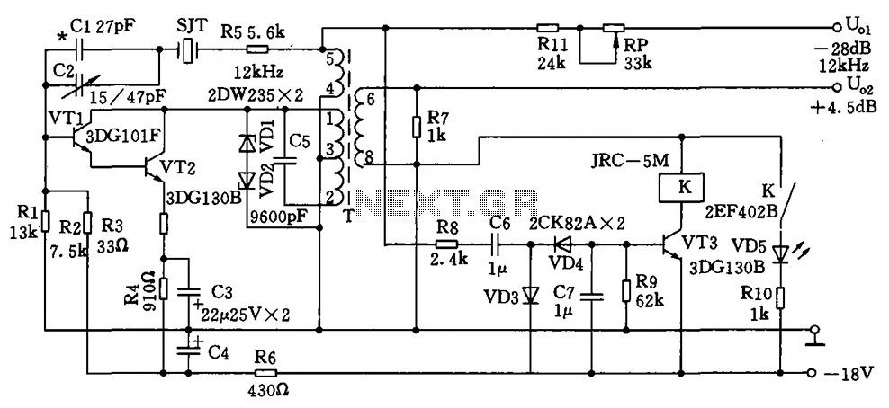
The circuit depicted is a 12 kHz intermediate frequency oscillator designed for an alarm system. It employs a variable feedback oscillation circuit where the oscillation frequency is primarily determined by a quartz crystal. Capacitors C1 and C2 are used...
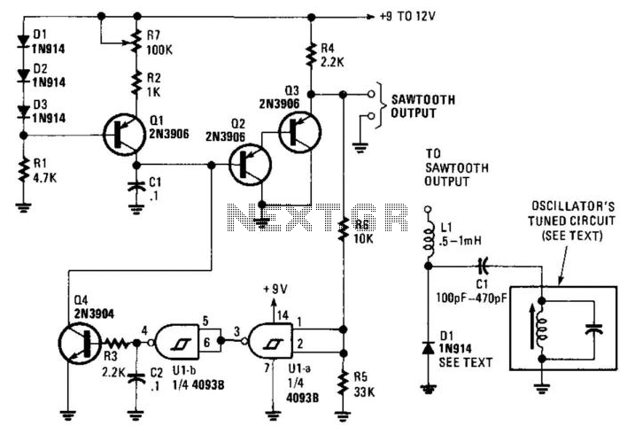
This circuit generates a linear sawtooth waveform with a frequency range from 30 Hz to 3,000 Hz. Q1 acts as a constant-current source that charges capacitor C1 until the output level at the emitter of Q3 triggers operational amplifiers...
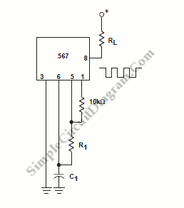
Unique applications of the 567 tone/frequency decoder IC include its use as a pulse generator with a 25% duty cycle. This signal generator produces... The 567 tone/frequency decoder IC is a versatile component widely used in various electronic applications, particularly...
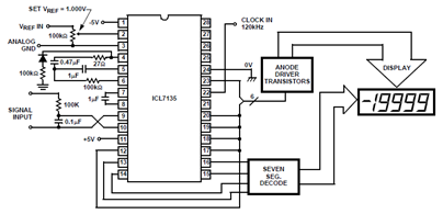
The schematic below shows the ICL7135 integrating analog-to-digital converter (ADC) functional diagram. According to the datasheet, an integrating converter is the right choice for panel meters and digital voltmeter applications. It can also be used for reducing line frequency...
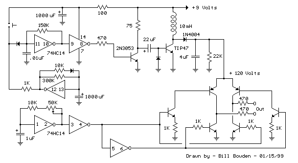
The telephone ring generator illustrated below produces the necessary high voltage using a simple switching mode power supply (SMPS) that incorporates a CMOS Schmitt Trigger square wave oscillator, a 10 mH inductor, a high voltage switching transistor (such as...
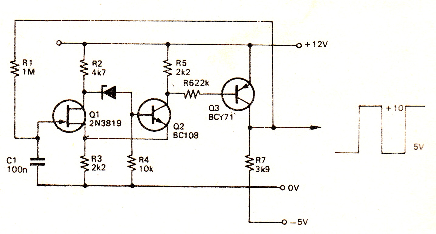
The circuit employs a field-effect transistor (FET) at the input of a Schmitt trigger, allowing the use of a low-value capacitor. The trigger, controlled by Q1 and O2, exhibits a hysteresis of approximately 3V, regulated by a 3V zener...