
Simple Square Wave Generator Circuits
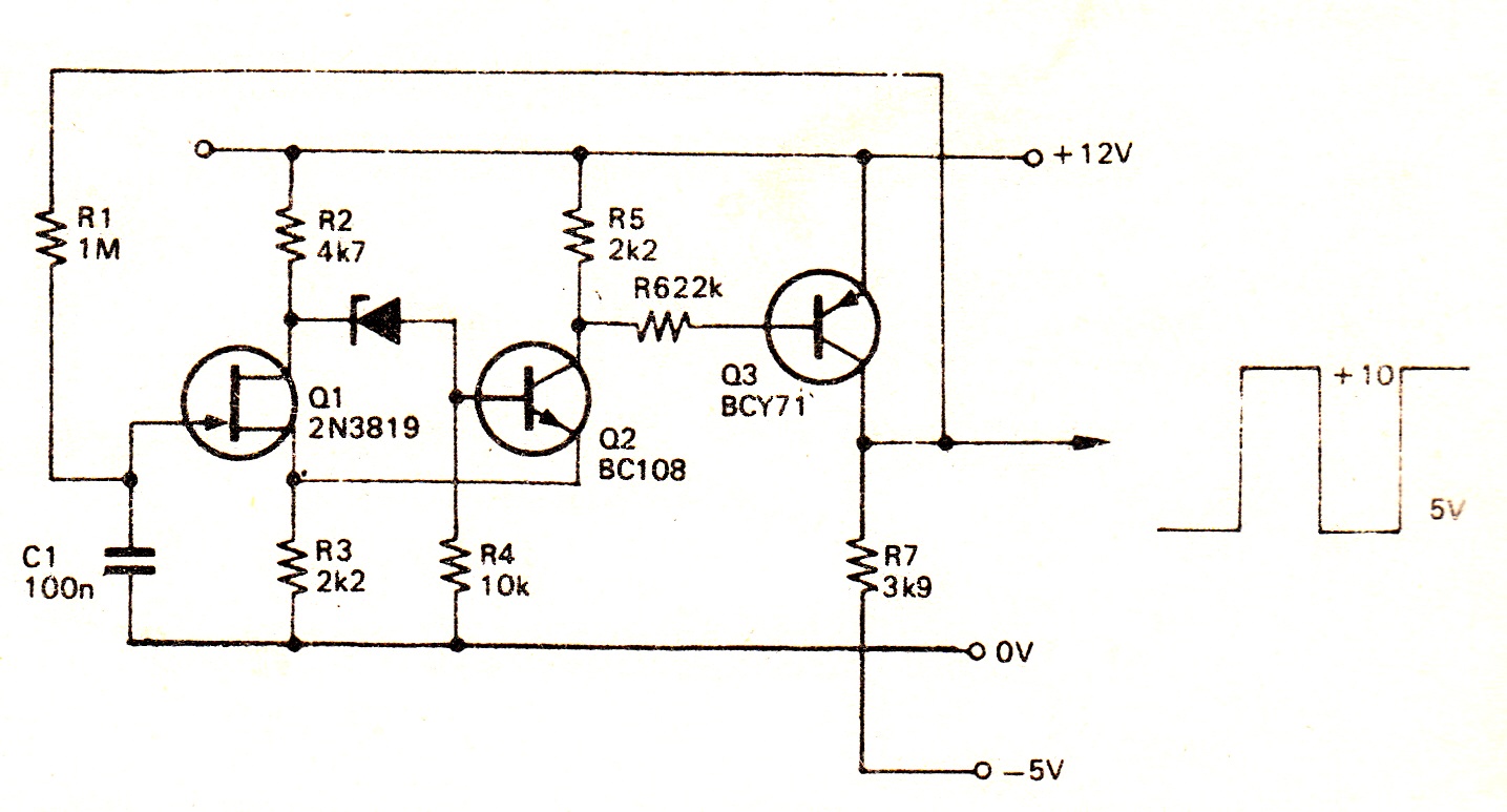
The described circuit utilizes a field-effect transistor as the primary input element to a Schmitt trigger configuration, which provides enhanced noise immunity and a defined switching threshold. The hysteresis introduced by the combination of Q1 and O2 ensures stable operation by preventing false triggering due to noise or signal fluctuations. The integration of a 3V zener diode serves a critical role in regulating the voltage levels, allowing for precise control over the switching characteristics of the transistors involved.
The charging and discharging behavior of capacitor C1, governed by resistor R1, is pivotal in determining the oscillation frequency of the circuit. The time constant, given by the product of resistance and capacitance, dictates how quickly the capacitor can charge and discharge, thereby influencing the overall performance of the waveform generator. The LM3900N amplifiers are particularly advantageous for this application, as they can handle a variety of frequencies and facilitate the design of more complex oscillators.
The output characteristics, with a 50% duty cycle, are crucial for applications requiring precise timing signals. The ability to adjust the duty cycle by modifying R7 allows for flexibility in output signal behavior, accommodating different operational requirements. Furthermore, the use of a potentiometer for R1 provides additional tuning capabilities, enabling fine adjustments to the time constant and thereby the oscillation frequency.
The circuit's design also highlights the importance of feedback mechanisms in ensuring rapid transitions between states, which is essential for applications requiring sharp and reliable switching. The interaction between Q1, Q2, and Q3, facilitated by positive feedback, ensures that once the circuit transitions to a new state, it does so swiftly, minimizing the time spent in intermediate states that could lead to instability. Overall, this circuit exemplifies a robust approach to generating low-frequency square wave signals with adjustable characteristics, suitable for a range of electronic applications.Using a field effect transistor at the input of a schmitt trigger, means a low value capacitor can be employed. The trigger by Q1 and O2 has a hysteresis of approximately 3V. This is controlled by the 3V zenen Mth C1 uncharged O1 is off and O2 is forward biased. The voltage at the source of Q1 is approximately +4V. O2 conducts, thus turning on TR 3. The output is therefore at +1OV. C1 then charges via R1 and the gate voltage of Q1 goes positive. When the gate voltage is sufficiently positive Q1 conducts, turning off Q2. The positive feedback from the emitter of (12 to the source of (11 ensures a rapid switch off. Q3 also switches off and the output goes to -5V. Capacitor C1 now discharge towards -5V, but when the voltage across C1 falls by approximately 3V, Ol ceases to conduct, turning on 0. 2. The collector load of Q3 is connected to a negative supply giving a 50% duty cycle. (The circuit still oscillates if R7 is connected to GV but the duty cycle will change, the output remaining at OV for a longer period than at +10V).
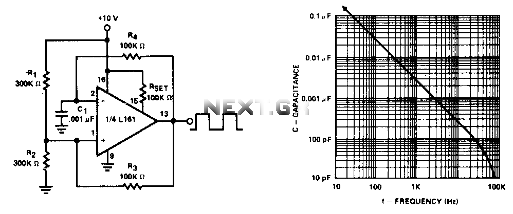
With the components as shown the frequency of the output is approximately 0. 025Hz. The multiple amplifiers in the LM3900N device are very suitable for use ln waveform generators at frequencies of up to about 10 kHz. Voltage controlled oscillators (the frequency of which is dependent on an input voltage) can also be designed using the device.
A simple square wave generator is shown. The capacitor Cn alternately charges and discharges between voltage limits which are set by R2, R 3 and R4. The circuit is basically of the Schmitt trigger type, the voltages at which triggering occurs being approximately Vt/3 and 2V+/ 3.
The time constant T of this circuit is equal to 0. 7 R;C2. Where T is in seconds, R1 in ohms and C2 in farads. For example when R1 = 10 k and C2 = 100 microfareds the time constant will be one second. Capacitor C2 may be selected over wide a range and Ry may be a potentiometer 100 k maximum. Outputs 1_and 2 provide pulses of opposite polarity but the rise time of output 2is long due to the charging current of C2. 🔗 External reference
Related Circuits
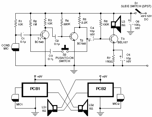
The circuit comprises a 3-stage resistor-capacitor coupled amplifier. When ring button S2 is pressed, the amplifier circuit formed around transistors T1 and T2 gets converted into an asymmetrical astable multivibrator generating ring signals. These ring signals are amplified by...
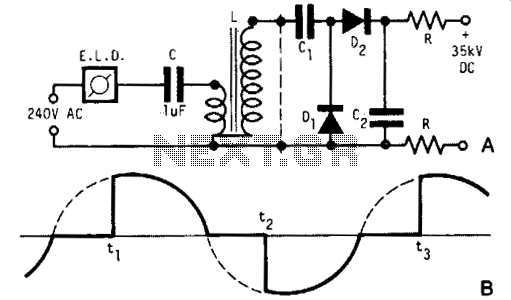
A light dimmer, a 1 µF capacitor, and a 12 V car ignition coil form a simple line-powered high-voltage generator. The current in the dimmer is illustrated in Fig. B. During the time intervals tp to t2, determined by...
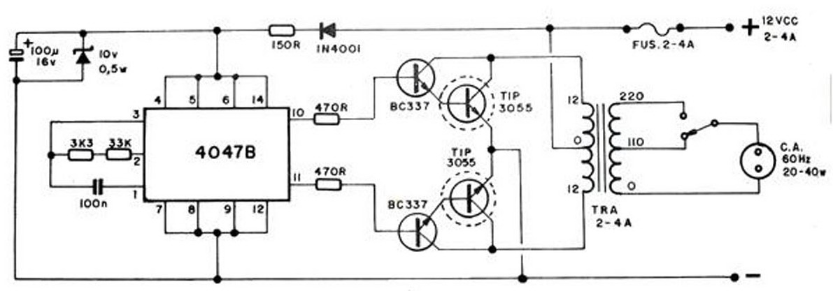
The converter transforms 12 VDC to 220 VAC, allowing for the conversion of 12 volts DC into 220 volts AC. The circuit diagram provided illustrates a simple converter circuit. This DC to AC converter can supply voltage for a...
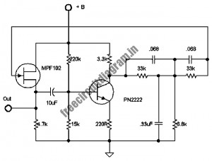
This generator operates at frequencies exceeding 100 kHz. The lower frequency limit is determined by capacitor Cl. Additionally, the frequency remains constant for supply voltages down to +5 V. The generator described is a versatile electronic oscillator capable of producing...
The following circuit illustrates a stable 60 Hz frequency signal generator circuit diagram. Features include a 0.068 µF capacitor incorporated within a feedback loop, allowing for DC-to-AC conversion. This circuit is designed to generate a stable 60 Hz sine wave...
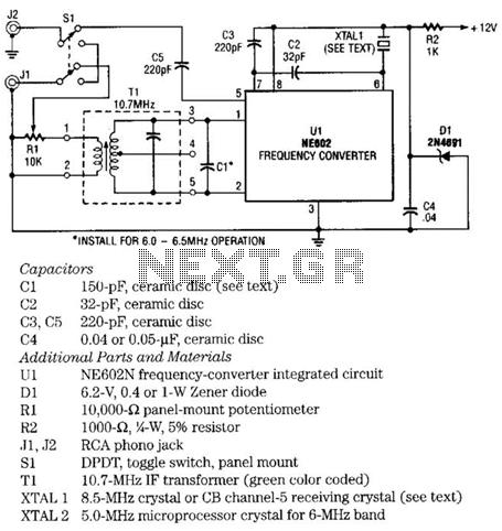
The NE602 chip, U1, contains oscillator and mixer stages. The mixer combines the oscillator signal with the input RF signal to produce signals whose frequencies are the sum and difference of the input frequencies. For example, an 8.5-MHz oscillator...