
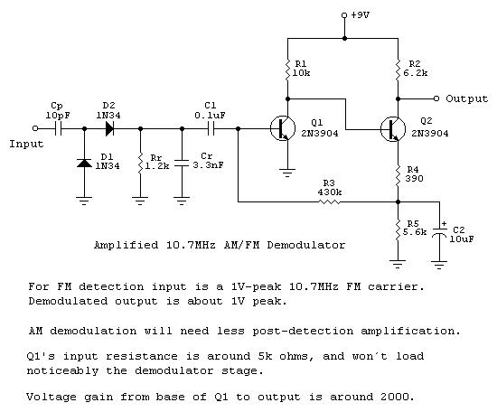
Diode Charge Pump AM-FM Demodulators
In this analysis, the DCP is examined under AC sine-wave excitation. The circuit is modeled as a voltage doubler driven by a periodic train of single-polarity pulses, each with a 50% duty cycle. This scenario can be represented by a switch that alternates between a battery providing V1 volts and a resistor R1 connected to ground. The switch remains in each position for equal durations. When positioned at "a," a pulse of height V1 is applied to capacitor Cp, which distributes its charge between capacitor Cr and resistor Rr. At the end of this pulse, Cp discharges through R1 and diode D1, while diode D2 remains non-conductive during this interval. Consequently, Cr discharges through resistor Rr. When the switch returns to position "a," the cycle repeats. If the pulse rate is sufficiently high, Cr's discharge will be incomplete during each cycle, resulting in a continuous current through Rr. The charge received by Cp per pulse is denoted as q1, the charge transferred to Cr as q2, and qr represents the charge that diverts through Rr (the portion of q1 that does not reach Cr). A linear relationship is established between the output voltage Vo and the pulse rate f, as well as between the output and the amplitude V1 of the input pulses. Thus, the DCP functions effectively as both an AM and FM demodulator.
Testing of the DCP with AM and FM modulated AC sine-wave inputs demonstrated successful recovery of the modulating signals. Therefore, it is beneficial to analyze the demodulation process under these new input conditions. The sine-wave excitation indicates that the circuit can be viewed as a half-wave voltage doubler. If the source voltage Vg has an amplitude V1 and frequency f, the steady-state output voltage for the unloaded case will be vo = 2V1. In this scenario, capacitor Cp charges to V1 volts. Upon connecting a resistive load Rr, the output voltage vo will no longer be purely DC; it will exhibit a DC component Vo with superimposed ripple. Diode D2 conducts briefly near the positive peaks of Vg, transferring charge from Cp to Cr, which subsequently discharges across Rr when D2 is off—this occurs for most of the interval between the positive peaks of the input voltage. Capacitor Cp replenishes its charge when diode D1 conducts briefly near the negative peaks of Vg. Consequently, vo will exhibit some ripple, along with the voltage across Cp.
The DCP circuit can be designed with specific components to optimize its performance. Key elements include the selection of diodes D1 and D2, which should have fast switching characteristics to minimize losses during the charge transfer process. Capacitors Cp and Cr should be chosen based on the expected load conditions, with capacitance values that ensure adequate charge storage and transfer efficiency. Resistor Rr must be selected to match the desired output load, balancing the trade-off between output voltage stability and ripple. The overall design should also consider the frequency range of operation, ensuring that the circuit can effectively demodulate both AM and FM signals across the intended bandwidth. Proper layout techniques, including minimizing parasitic inductance and capacitance, are essential for maintaining signal integrity and achieving optimal performance in real-world applications.Frequency-to-voltage converters form part of a wide variety of instrumentation circuits. They also find use in radio as FM demodulators. One interesting configuration for this application is the Diode Charge Pump circuit (DCP), which also doubles as an AM detector. The DCP is basically a pulse-driven half-wave voltage doubler. Its use as a demodulator derives from the analysis of charge transfer taking place between circuit components.
In this article I will attempt to explain why the demodulation process takes place in the DCP. Following, the circuit will be studied under AC sine-wave excitation. Let s begin then analysing a voltage doubler driven by a periodic train of single-polarity pulses having a duty cycle of 50% (Fig. 1. a). We shall model this situation by a switch that toggles between a battery delivering V1 volts and a resistor R1 connected to ground (Fig.
1. b). The switch stays in each position equal periods of time. When the switch is in position "a" a pulse of height V1 is applied to Cp. The charge received by this capacitor is distributed between Cr and resistor Rr. At the end of the pulse, Cp discharges through R1 and D1 (switch in position "b"). Diode D2 does not conduct (is an open circuit) on this interval. As a consequence, Cr discharges through Rr. When the switch returns to the "a" position, the operation cycle is repeated. If the pulse rate is sufficiently high, Cr`s discharge will be incomplete on each cycle and a continous current will flow through Rr. Here, q1 is the charge received by Cp per pulse; q2 is the charge transferred to Cr, also per pulse (it restores the charge lost by this capacitor in the preceding cycle) and qr is the charge that diverts through Rr (fraction of q1 that doesn t reach Cr).
Clearly, a linear relationship exists between Vo and the pulse rate f, and also between the output and the height V1 of the input pulses. The output linearly follows any frequency or amplitude input changes. Hence, the DCP may act as an AM/FM demodulator. The DCP was subjected to tests with AM and FM modulated AC sine-wave inputs. In each case, successful recovery of the modulating signal could be achieved. It has then been found advisable to analyse the demodulation process with these new input conditions.
Sine excitation suggests that it is best to look at the circuit as being a half-wave voltage doubler. With this in mind, if the source voltage Vg has an amplitude V1 and frequency f, then for the unloaded case the steady-state output voltage will be vo = 2V1.
Note that capacitor Cp will be charged to V1 volts (Fig. 2. a). Upon connection of a resistive load Rr (Fig. 2. b), the output voltage vo will no longer be a pure DC value. It will consist of a DC component Vo and some ripple superimposed on it. D2 will conduct for a brief time in the neighborhood of the positive peaks of Vg, transferring charge from Cp to Cr. This last capacitor discharges across Rr when D2 is off, which occurs during most of the time interval between positive peaks of the input voltage.
Cp replenishes its charge when D1 briefly conducts in the neighborhood of the negative peaks of Vg. As a result of these actions vo will have some ripple added, as stated before, and also will the voltage across Cp. 🔗 External reference
Related Circuits
The Accu charger circuit is straightforward and simple to construct, requiring no more than ten components. In addition to its ease of assembly, this charger circuit is also cost-effective and highly efficient. The circuit requires a power supply from...
A battery is a vital element of any battery-backed system. In many cases, the battery is more expensive than the system it is backing up. Hence, practical measures must be adopted to conserve battery life. As per manufacturer's data...
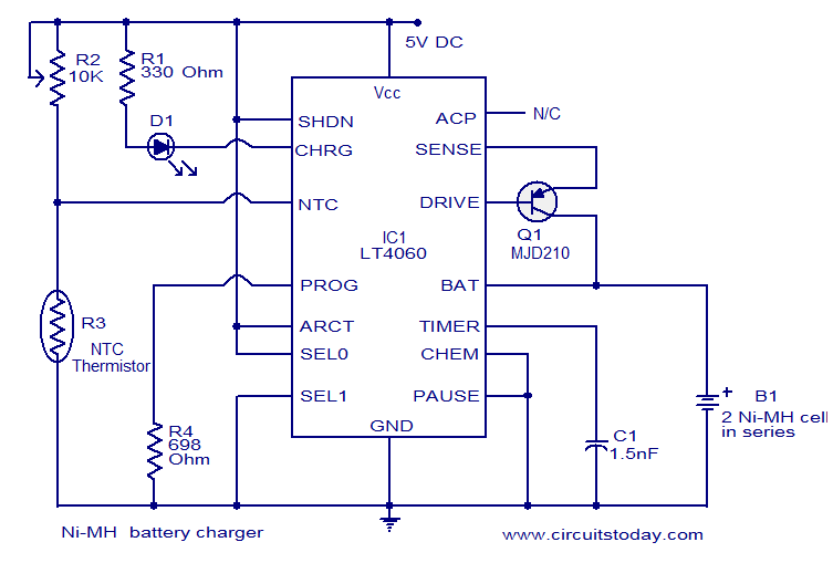
This circuit diagram represents a highly efficient Ni-MH battery charger utilizing the LT4060 integrated circuit from Linear Technologies. The circuit can also accommodate Ni-Cd batteries with minor modifications. To charge Ni-Cd batteries, the CHEM pin (pin 12) of the...
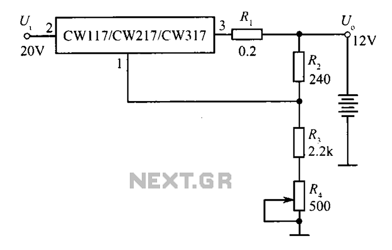
A 12V constant voltage charger is depicted. The power supply circuit shares the same basic design. The resistor R1, valued at 0.2 ohms, serves a limiting function, effectively increasing the internal resistance of the charger, which in turn reduces...
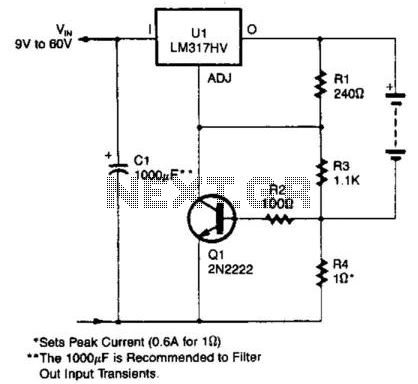
An LM317HV regulator is utilized as a current-limited charger. If the current through R4 exceeds 0.6 A, Q1 is activated, which pulls the ADJ terminal of the LM317HV to ground and reduces the battery charging current. The LM317HV is...
This circuit illustrates a Lithium Battery Charger circuit diagram. Charging is achieved using a constant current of 60 mA for AA cells until a cutoff voltage of 2.4V per cell is reached, at which point the charging process must...
Warning: include(partials/cookie-banner.php): Failed to open stream: Permission denied in /var/www/html/nextgr/view-circuit.php on line 713
Warning: include(): Failed opening 'partials/cookie-banner.php' for inclusion (include_path='.:/usr/share/php') in /var/www/html/nextgr/view-circuit.php on line 713