
discussing output stage of square wave
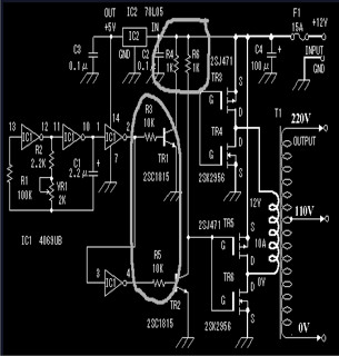
The circuit design incorporates critical resistors that influence the performance and stability of the transistors and MOSFETs. The 10K resistors at the transistor bases serve to limit the base current, ensuring that the transistors operate within safe limits and preventing damage. Likewise, the 1K resistors at the collectors are vital for the proper operation of the MOSFETs, as they help manage the voltage and current flowing through the devices, ensuring reliable switching.
The oscillator section is designed to generate a waveform that can be adjusted based on the circuit's requirements. The output stage is responsible for amplifying this waveform and driving the transformer, which is crucial for applications such as power inverters. The design retains the integrity of the square wave format, which is known for its efficiency in driving inductive loads.
The inquiry about the diode junction and the potential removal of resistors R4, R5, R6, and R7 suggests a simplification of the circuit to enhance performance. By connecting the diode junctions directly through the 10K resistors, it may be possible to reduce complexity while maintaining functionality. However, caution is advised, as any changes made to the circuit, particularly in the secondary winding, could lead to unforeseen issues, including component failure and operational instability.
In summary, the circuit's performance hinges on the careful selection and placement of resistors and other components. Maintaining the integrity of the original design while making adjustments is critical to achieving the desired operational characteristics and ensuring reliability in the overall system.What about the 10K resistors at the bases of the transistors, and the 1K resistors at the collectors. Keep those with theTransistors when I move them, orget rid of them If the 10K resistors are not included the transistors will blow-off, without the 1K collector resistors the mosfets will not work.
so all of them are required. we are just interested in changing the waveform, which is solely connected with the oscillator section. The output stage which is responsible only for boosting the signals into the transformer windings, remains the same, just as it was with the square wave design. Hi Swag, one more question. On your circuit, at the Diode Junction, should I get rid of R4, R5, R6, R7 and just use the two 10K resistors, with the transistors.
Hi Swagatam, I followed your instructions to the letter and it still does not work. This time when I turned the Inverter ON it made a loud high pitched noise and blow one of the Mosfets. Sorry for the bad news. Hi Swagatam, here is a picture of the complete circuit on a PCB. The Square wave generator and PWM circuitare ontwo separate PCBs. I sure hope we can get this thing working. Quite unfortunate that its not working, you may directly connect the diode junctions through the 10K resistors of the square wave design, so R4, 5, 6, 7 are not required.
are you sure you are using exactly the same output stage set-up that was previously working with the square wave design I think you did some changes in the secondary winding. if that is true then that may be root cause of all the trouble. 🔗 External reference
Related Circuits
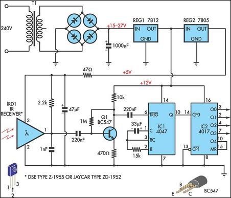
This circuit allows any infrared (IR) remote control to manage the outputs of a 4017 decade counter. It utilizes a 3-terminal IR receiver (IRD1) to capture infrared signals from the transmitter. The output from IRD1 is connected to an...
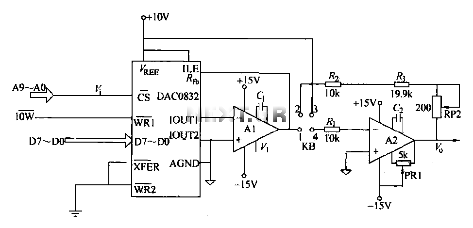
The DAC0832 is a digital-to-analog converter (DAC) chip designed for integration with computer bus systems. It features an 8-bit resolution and operates with a single power supply ranging from 5 to 15 volts. The device is compatible with TTL...
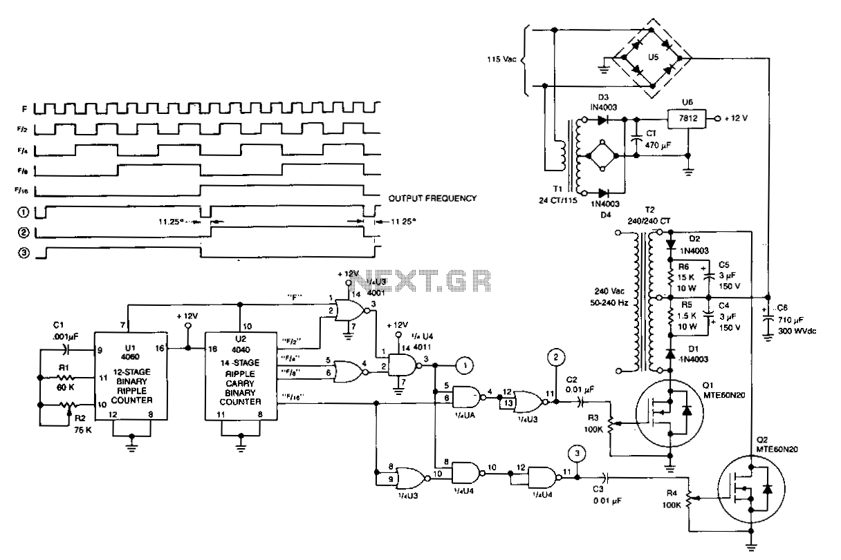
U1 is a 4060 12-stage binary ripple counter that operates as a free-running oscillator, with its frequency of oscillation calculated as 1/2.2 CIR2. The output from U1 is fed into U2, a 14-stage binary ripple counter that generates square-wave...
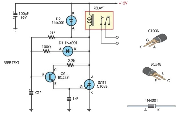
This circuit is designed to provide delayed relay switching action at power on. The delay is a function of the time constant produced by the combination of components. The circuit operates by utilizing a timing element, typically a resistor-capacitor (RC)...
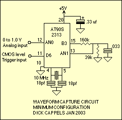
The approaches using on-chip A-to-D converters on AVR, PIC, and Cypress controllers reached sample rates of up to about 60 kHz. Not really very useful for the sort of thing I was thinking about using this for: encoded data,...
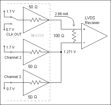
The NI 655X is a versatile high-speed digital product capable of interfacing with various technologies. This application note illustrates how to connect the NI 655X to Low Voltage Differential Signaling (LVDS) devices. LVDS is an emerging differential digital standard...