
Interfacing to LVDS with the NI 655X Digital Waveform Generator/Analyzer

The NI 655X is designed to facilitate the generation and analysis of LVDS signals effectively, leveraging its digital capabilities to interface with low voltage differential signaling technology. The ability to configure the output voltage levels and current appropriately is critical for ensuring reliable communication between devices. The integration of a 100-ohm terminating resistor at the receiver is essential for maintaining signal integrity, allowing for accurate voltage readings that align with LVDS specifications. Furthermore, the importance of maintaining proper impedance matching throughout the system cannot be overstated, as mismatched impedances can lead to signal reflections and degraded performance. The differential nature of LVDS allows for improved noise immunity and reduced electromagnetic interference, making it suitable for high-speed data transmission in various applications, including telecommunications and data acquisition systems. The NI 655X's flexibility in generating LVDS signals opens up a wide range of possibilities for engineers and designers looking to implement high-speed digital communication in their projects.The NI 655X is a versatile high-speed digital product that can interface to many different technologies. This application note shows how to interface the NI 655X to LVDS devices. Low Voltage Differential Signaling (LVDS) is an emerging differential digital standard used in several communication and mixed-signal applications.
The electrical charact eristics of an LVDS signal can facilitate significant performance improvements compared to single-ended standards. For example, since the received voltage is a differential between two signals, the voltage difference between the logic high level and low level state can be small, allowing for faster rise and fall times.
Another unique characteristic of LVDS is that it is a current-driven technology. Therefore, you must ensure your application has the correct termination and current-return paths. A current source at the driver provides approximately 3. 5 mA of current. The direction of the current across the transmission line depends on whether the driver is driving a logic high level or low level. When the current reaches the receiver, a 100 © terminating resistor connects the two ends of the transmission line to provide a return path for the current.
In addition, a voltage of approximately 350 mV is established across the two input terminals of the differential receiver. This differential voltage is either positive or negative, depending on the direction of the current. Based on the polarity of the voltage, the receiver recognizes the signal as either a high or low level.
As discussed in the introduction, LVDS is a differential, current-driven technology. The 655X, on the other hand, is a single-ended, voltage-driven digital waveform generator and analyzer. However, the flexibility of the 655X family of products allows you to easily interact with LVDS devices.
You can easily generate LVDS signals using two DIO channels to generate the two ends of the differential signal. The 655X devices have a 50 © source impedance on their output terminals that must be considered when configuring the voltage levels of a generation operation.
The NI 655X generation voltage levels must be set so that the appropriate current and voltage are seen at the receiver. Setting the generation voltage high level and generation voltage low level to 1. 7 V and 0. 7 V, respectively, works well. Those settings cause 5 mA to flow through the circuit, causing a voltage of 500 mV at the receiver (see Figure 3).
The LVDS specification allows for an input voltage range from 0 to 2. 4V, so a wide range of acceptable values are available. The common-mode voltage seen at the receiver in this case is 1. 2 V, which is within the ideal range for LVDS. Programming the 655X to perform this generation is similar to programming a regular single-ended operation. As shown in figure 4, two channels are configured for generation. After you set the clock rate, set the voltage levels to the appropriate values, and then the device downloads the waveform.
Notice that the data for the two channels are always inverse of one another. Another product, the NI 5421 is also capable of generating 16 channels of LVDS output. Either of the two higher memory options of the 5421 have this capability. See NI 5421 link at the bottom of this page for more information. For an example of what happens if the correct settings are not used, assume both ends of an LVDS signal were wired directly to two input terminals on the NI 655X, each with 50 © input impedance. The circuit would look like Figure 5. In this example, the driver`s constant current source attempts to push 3. 5 mA through the positive wire. With a 50 © terminating resistor to ground, the voltage at the receiver is 175 mV, well below the desired LVDS common-mode voltage of 1.
2 V. The negative leg is pulled to ground by the other 50 © resistor, forcing the voltage to be 0 V. Many LVDS drivers consider this to be an open-fault co 🔗 External reference
Related Circuits
%2Bwith%2Banimation%2Bsimulation%2Bcircuit.png)
The Johnson digital counter, also known as the Twisted Ring Counter, is a synchronous shift register that incorporates feedback from the inverted output (Q`) of the last flip-flop. The Q` output of the final flip-flop is connected back to...
The BU8872 and BU8872FS are DTMF receiver integrated circuits designed for application in telephone answering machines, converting 16 distinct types of DTMF signals into 4-bit binary serial data. These receivers are available in a compact 8-pin DIP package (BU8872)...
The digital sine wave generator (oscillator) circuit requires only a few components to produce signals with high amplitude constants and a wide range of variable frequencies. This circuit generates a sine wave signal, and by altering the values of...
The digital display temperature detection circuit utilizes a precision digital display to indicate temperature readings. The circuit employs the MC1403, which outputs a reference voltage, with the potentiometer RP5 setting the reference value for the inverting terminal (a) of...
This document serves as a resource for developers who are new to Texas Instruments (TI) ARM-based processors, as well as for seasoned developers seeking to deepen their understanding of the different ARM architectures. It starts with an overview of...
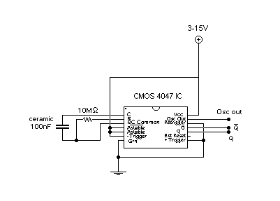
This circuit provides a digital square wave that can be viewed directly or used to drive other circuits. It used the CMOS 4047 Low-Power Monostable/Astable Multivibrator. As used in Tom Duncan's Adventures with Digital Electronics Book, to drive CMOS...