
Divide-By-2-Or-3 Circuit
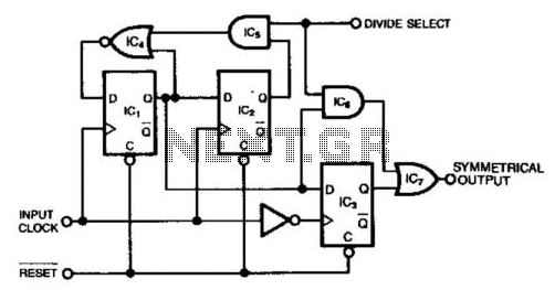
The circuit operates based on a combination of digital logic components including flip-flops and gates. The primary components involved are two flip-flops (IC1 and IC2), which are configured to provide division by 3 when the Divide Select signal is high. This is achieved through a feedback mechanism that involves the AND gate (IC5) and the NOR gate (IC4), which together control the state of IC1.
When the Divide Select input is low, the circuit transitions to a divide-by-2 configuration. The AND gate IC5 outputs low, causing the NOR gate IC4 to invert the feedback signal, which in turn toggles the state of IC1. This configuration allows IC1 to function as a toggle flip-flop, effectively altering the output frequency to half the input frequency.
IC3 plays a crucial role in generating symmetrical output signals. It is designed as a negative-edge-triggered flip-flop, which means it responds to the falling edge of the clock signal. When the circuit is set for division by 2, IC3's output is simply a delayed version of its input, maintaining the integrity of the signal while providing the necessary timing adjustments.
When the circuit is switched to divide by 3, the output path through gates IC6 and IC7 becomes active. This allows the output to respond to the leading edge of the input signal from IC3, rather than the output itself. The result is a symmetrical divide-by-3 output, which is essential for applications requiring precise timing and waveform generation.
In summary, this circuit effectively utilizes flip-flops and logic gates to achieve frequency division by 2 or 3, providing a versatile solution for applications that demand symmetrical waveforms at different frequency ratios. The careful design of the feedback and control mechanisms ensures reliable operation across both division modes. This circuit produces a symmetrical waveform when dividing by either 2 or 3. The Divide Select input controls the division factor. When Divide Select is high, flip-flops IC1 and IC2, along with associated gates, form the classical divide-by-3 circuit. When divide select is low, however, the output of the AND gate, IC5, goes low. Consequently, the NOR gate, IC4, inverts the feedback signal and passes it to the D input of the flip-flop, IC1.
Now, IC1 acts like a toggle flip-flop and produces a divide-by-2 output. IC3, which is, in effect, a negative-edge-triggered flip-flop, provides symmetrical output signals. When you select division by 2 (Divide Select is low), the output and AND gate IC6 is low, and IC3 simply clocks out the divider"s output, delayed by one clock period. When you set Divide Select high, the path to the output through the AND and OR gates, IC6 and IC7, is enabled.
This path means that the output goes high on the leading edge of IC3"s input (not its output) and produces a symmetrical divide-by-3 output. 🔗 External reference
Related Circuits
A printed circuit board (PCB) was presented along with a schematic detailing the arrangement of components required for the activation of an LED on the board. The purpose of the PCB is to facilitate planning for the eventual construction...
This design circuit is for a mass air flow (MAF) sensor. The MAF sensor converts the volume of air entering the engine into a voltage signal. The main components of the MAF sensor include a thermistor, a platinum hot...
When working with these circuits, a light meter was purchased to eliminate the uncertainty in assessing light levels, as the human eye is not very reliable for this purpose. In electronic circuit design, particularly when dealing with light-sensitive applications, the...
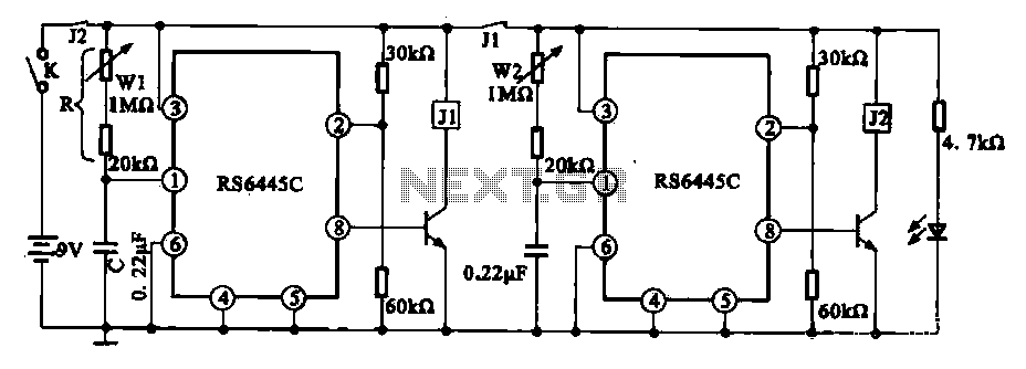
The timing integrated circuit (IC) RS6445C functions as a blocking oscillator. It features two segments, WI and W2, which are utilized to adjust the working time and the closure time. These adjustments can be continuously set within a range...
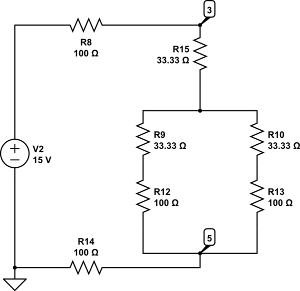
The Delta configuration of resistors R2, R3, and R4 is converted to a Wye (Y) configuration. This conversion is necessary because a voltage divider is typically employed in series circuits. The aim is to determine the total resistance in...
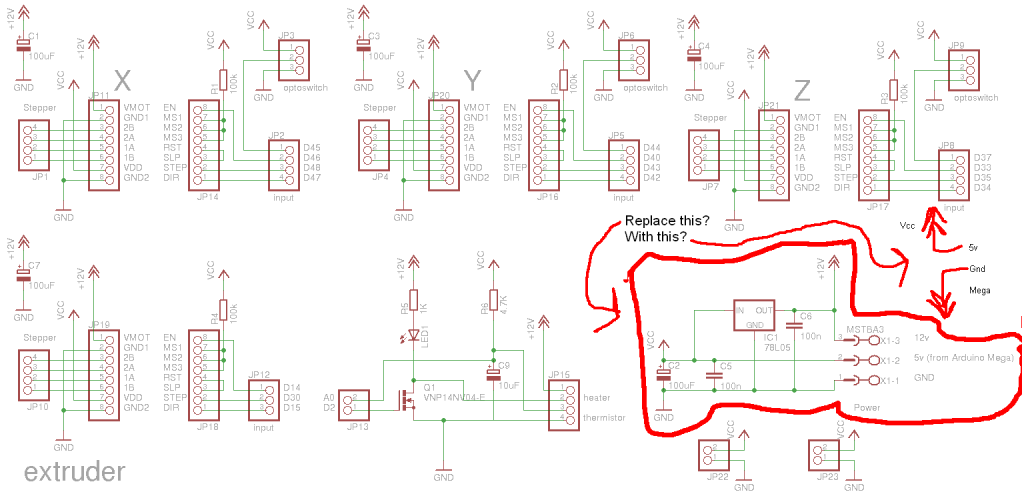
Preparing to assemble Adrian's Pololu stepper driver circuit has raised a question. He indicates that if using 5V from the Arduino Mega, the 78L05 voltage regulator should be omitted. This is a positive development, although there is an incorrect...