
DTL internal structure of the inverter circuit

The M5936P DTL (Diode-Transistor Logic) inverter circuit utilizes a combination of diodes and bipolar junction transistors (BJTs) to perform its logical operations. The circuit is powered by a +5V supply, which is standard for digital logic circuits, ensuring compatibility with other digital components.
In the high input state, where terminal A receives a logic high (digital 1), diode VDI becomes reverse-biased, preventing current flow through it. Concurrently, this condition allows transistor VT1 to turn on, which then drives the base of transistor VT2. As a result, transistor VT2 enters saturation, allowing current to flow from the collector to the emitter, thus producing a low output state (digital 0) at the output terminal.
In contrast, when the input state is low (digital 0), diode VD1 becomes forward-biased, allowing current to flow through it. This action turns off transistor VT1, which in turn keeps transistor VT2 in the off state as well. Consequently, the output terminal reflects a high state (digital 1), indicating that no current flows through the output.
This inverter circuit exemplifies the fundamental operation of DTL logic, where the combination of diodes and transistors effectively implements logical inversion. The design is efficient for small signal processing applications and can be integrated into larger DTL logic families for more complex digital systems. The simplicity of the inverter circuit allows for easy expansion and incorporation into various digital applications while maintaining reliability and performance.DTL internal structure shown in the inverter circuit (M5936P) is. Inputs with diodes, transistors signal processing, power supply is + 5V. When the input terminal A high level (digital I ) when the diode VDI off, VTI transistor is turned on, the transistor VT2 conduction output is low (digital O ). When the input is low (the number 0 ), the diode VD1 conduction, transistor VT1 off, transistor VT2 off, output high (the number 1 ).
Related Circuits

The circuit illustrated here demonstrates that, despite advancements in components and technology, it remains possible to design effective and intriguing circuits. This design utilizes two well-known transistors, the BF256C and the BF494. Along with the necessary resistors and capacitors,...
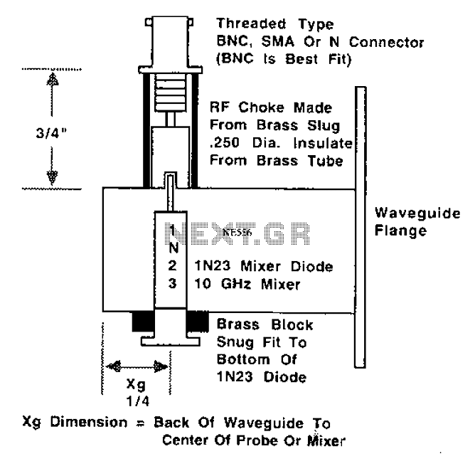
This is a 10 GHz frequency amateur radio waveguide detector. The 10 GHz amateur radio waveguide detector is designed to operate within the microwave frequency range, specifically targeting the 10 GHz band commonly used in various amateur radio applications. The...
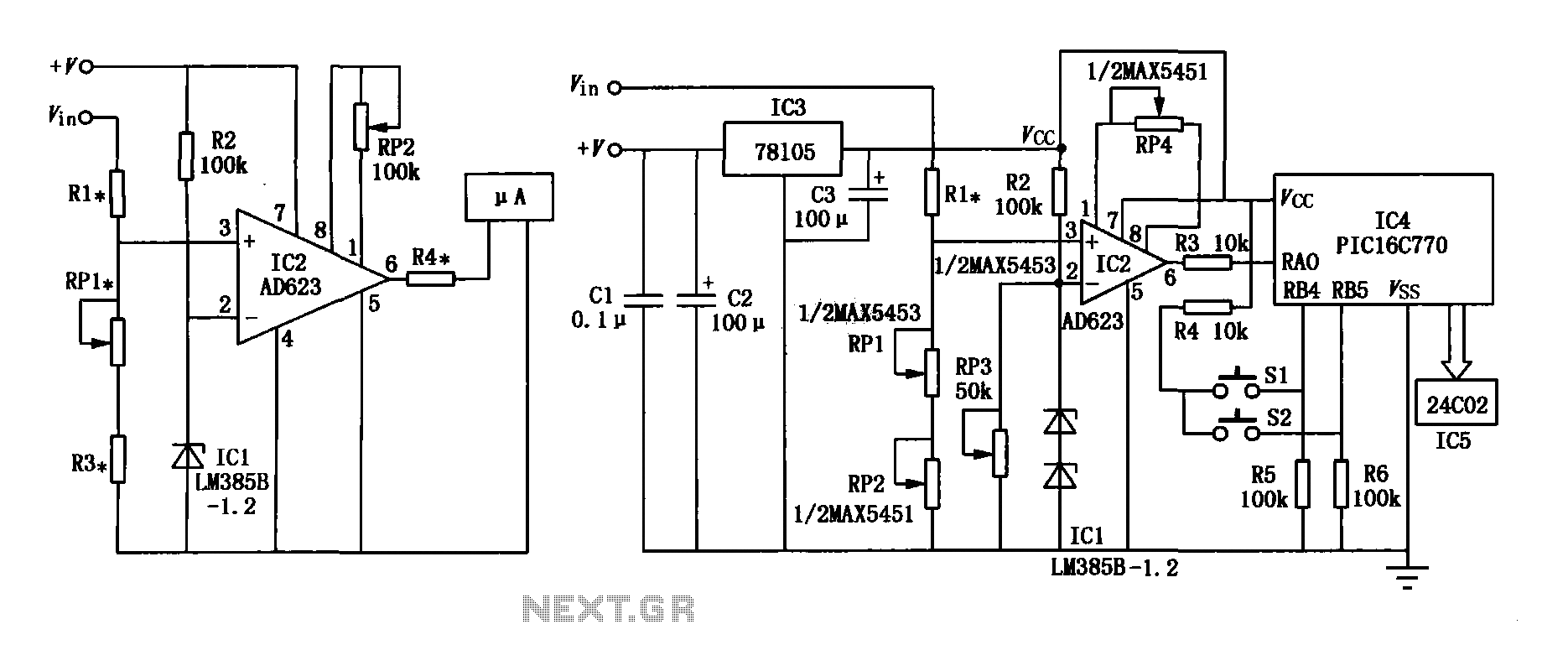
The range precision voltmeter electrical schematic is depicted in Figure (a) below. It features an amplifier circuit and several high-precision components that significantly enhance the performance range of the voltmeter. The inverting input of the instrumentation amplifier AD623 (IC2)...
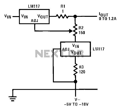
This circuit illustrates an adjustable regulator configuration that incorporates a voltage regulator. In this design, the LM117 regulator is utilized instead of the LM113 diode for reference. Both regulators necessitate a negative supply to function correctly with respect to...
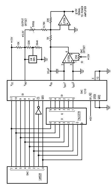
The LM628 and LM629 dedicated motion-control processors can be utilized to design various applications involving DC and brushless DC servo motors, as well as other servomechanisms. The power path of this electronic project, which functions as a motor driver,...
The HT6337 is an infrared remote control receiving decoder circuit specifically designed for electric fan applications. It is housed in a 28-pin dual-row DIP package, with the compatible model being HT12C. The HT6337 is part of a series of...