
Dual AC radio remote control switch circuit diagram
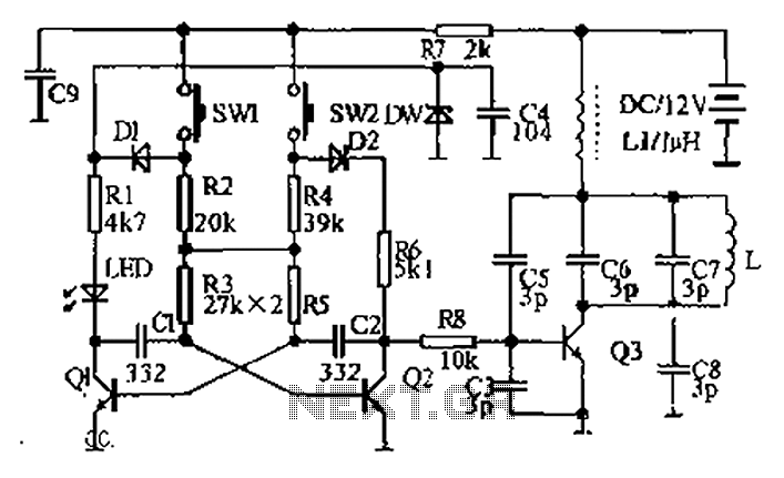
The dual radio remote control switch circuit operates effectively by utilizing a combination of oscillators and demodulators to manage multiple frequencies. The transmitter section is designed to generate distinct frequencies based on the switch pressed, allowing for versatile control options. The use of Q3 for high-frequency signal generation ensures reliable transmission over a distance, while the oscillator configuration with Q1 and Q2 enables quick frequency shifts between 5 kHz and 3.7 kHz.
The receiving section is critical for interpreting the transmitted signals. The demodulation process, facilitated by Q4 and Q5, ensures that the audio signals are accurately translated back into control pulses for the bistable circuits. The integration of IC1 and IC2 allows for simultaneous control of two distinct functions, enhancing the circuit’s functionality. The STA401A component plays a pivotal role as it manages the state of the output based on the received pulses, effectively controlling the load and enabling relay operations.
The TLP3503 optical coupling circuit serves as an interface between the low-power control signals and the higher power load, ensuring isolation and protecting sensitive components from voltage spikes. This design choice enhances the reliability and safety of the circuit during operation. The overall architecture of the dual radio remote control switch circuit exemplifies efficient design practices in remote control applications, providing both functionality and ease of use. As shown in FIG AC is a dual radio remote control switch circuit. Transmitter: Q3 generates a high frequency carrier signal. Q1, Q2 composition oscillator circuit. When you pre ss SW1, the oscillation frequency of 5kHz, press SW2, the oscillation frequency is 3.7kHz. When the start-up circuit, LED as work instructions. Receiving circuit: Q4 and peripheral components receiving circuit, two demodulated audio signals, in pre-release Q5, and then into IC1, IC2 of 3 feet. IC1 demodulation frequency 5kHz, the corresponding transmitter SW1, IC2 correspond SW2.SW1 when pressed, IC1 8-pin switch sends a pulse when SW2 is pressed, IC2 pin 8 also sends switch pulses.
Two pulses are fed STA401A. STA401A and peripheral components of two separate bistable circuit. IC1 fed pulse to 4 feet STA401A goes low, TLP3503 (optical coupling circuit) input of a current flowing through the load electrical work. STA401A another way to control relay. Press the appropriate button, STA401A corresponding circuit reset.
Related Circuits
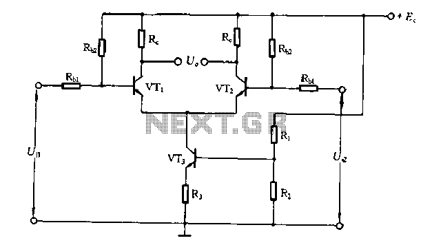
The differential amplifier circuit features a constant current source. The differential amplifier is a fundamental building block in analog electronics, utilized for amplifying the difference between two input voltages while rejecting any signals that are common to both inputs. Central...
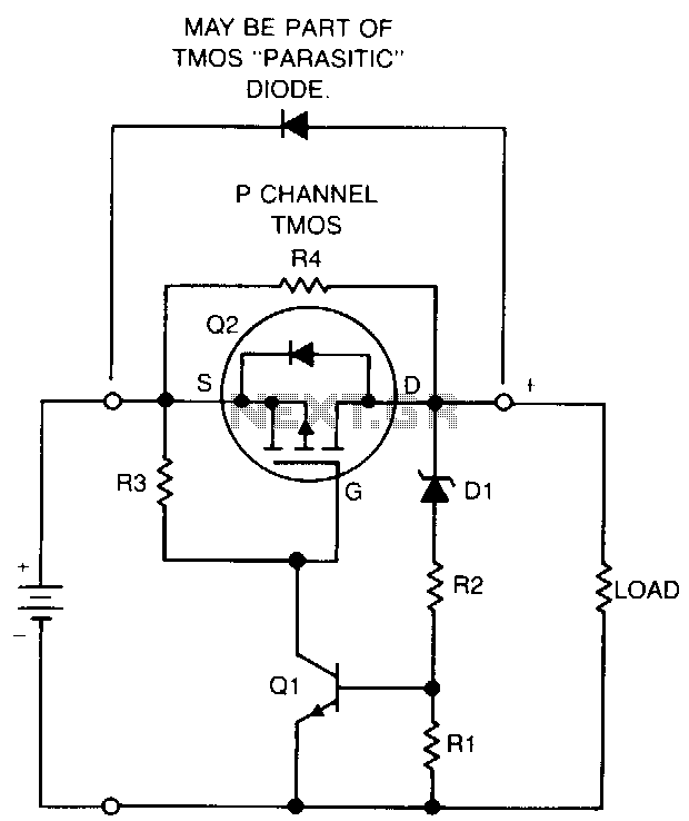
If a NiCad battery is discharged to the point where the lowest capacity cell becomes fully discharged and reverses polarity, that cell will typically short internally and become unusable. To prevent this type of damage, this circuit detects a...
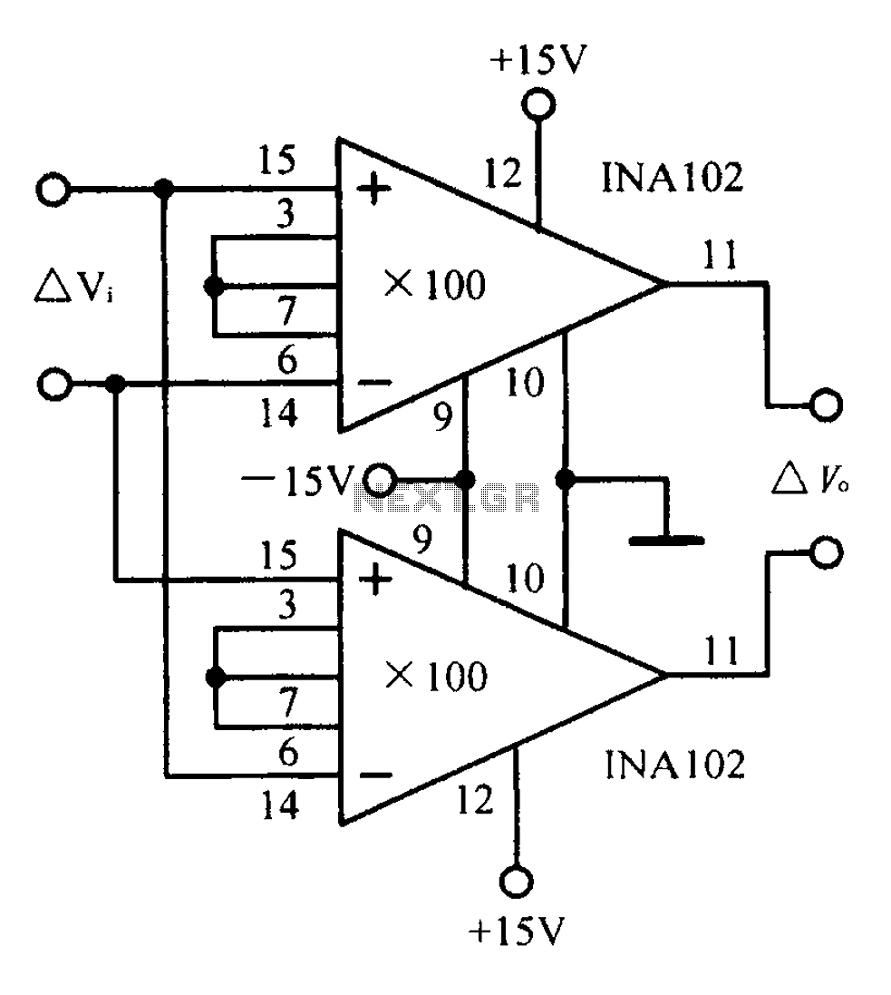
A differential input differential output amplifying circuit diagram. A differential input differential output (DIDO) amplifier is a type of operational amplifier configuration that is designed to amplify the difference between two input signals while rejecting any signals that are common...
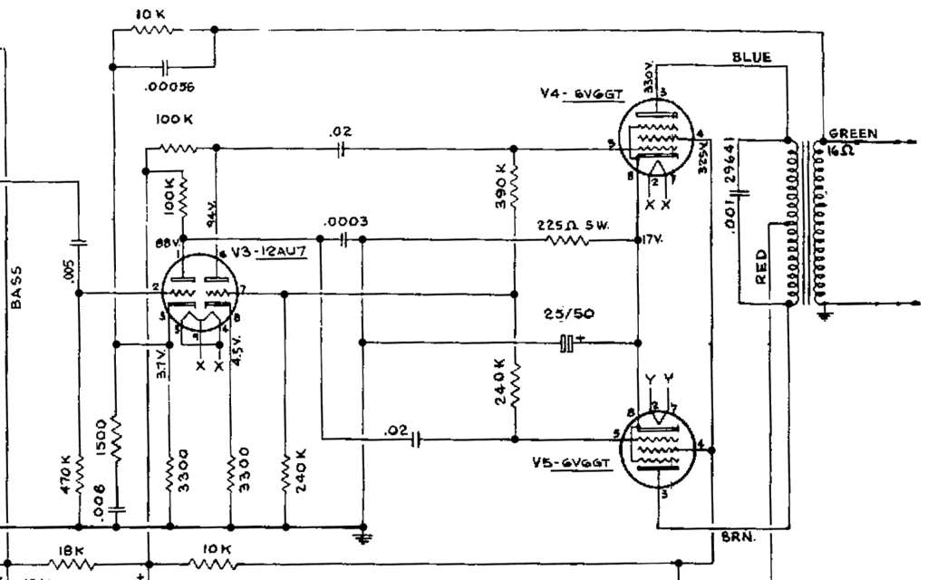
This schematic has been modified from an old Bell & Howell projector amplifier for model 302, utilizing PP 6V6 tubes with a 12AU7 phase inverter (PI). The PI circuit appears to be closest to a "floating paraphase." There is...
An automatic electric furnace temperature controller is illustrated. The closed circuit consists of a temperature detection output control loop; as the temperature increases, the output voltage rises until it reaches a preset temperature value, at which point the output...
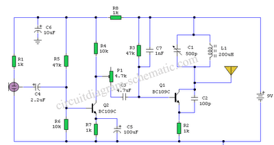
The AM transmitter circuit consists of an audio amplifier and an RF oscillator. The oscillator is constructed around transistor Q1 and its associated components. The tank circuit, which includes inductor L1 and variable capacitor VC1, is tunable from approximately...
Warning: include(partials/cookie-banner.php): Failed to open stream: Permission denied in /var/www/html/nextgr/view-circuit.php on line 713
Warning: include(): Failed opening 'partials/cookie-banner.php' for inclusion (include_path='.:/usr/share/php') in /var/www/html/nextgr/view-circuit.php on line 713