
Dual-Gate Mosfet Rf-Amp Stage
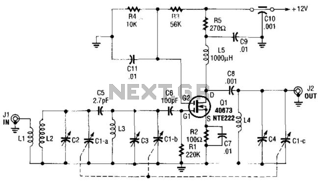
The circuit employs a double-tuned input stage, which enhances the selectivity of radio frequency (RF) signals by allowing the circuit to better discriminate between closely spaced frequencies. This configuration typically consists of two inductors and two capacitors, tuned to resonate at the desired frequency while providing a narrow bandwidth. The single-tuned output stage, in contrast, utilizes a single resonant circuit to extract the amplified signal, resulting in a simpler design but potentially reduced selectivity.
Incorporating Automatic Gain Control (AGC) into the circuit can improve performance by automatically adjusting the gain of the amplifier based on the strength of the incoming signal. In this design, the AGC is connected to gate 2 of transistor Q1, which is part of the amplification stage. The AGC circuit modulates the voltage applied to gate 2, driving it negative when higher gain is not needed. This negative bias effectively reduces the amplification, preventing distortion and ensuring that the output signal remains within optimal levels, even when faced with strong incoming signals.
The overall design benefits from the combination of double-tuned input and AGC, providing a robust solution for RF applications requiring high selectivity and stable gain control. This configuration is particularly useful in communication systems where signal integrity is paramount, allowing for improved reception and clarity in the presence of competing signals. The use of a double-tuned input and a single-tuned output yield superior RF selectivity to that of equivalent single-tuned designs. AGC, if required, can be added to gate 2 of Ql, and should drive gate 2 negative for decreased gain. 🔗 External reference
Related Circuits
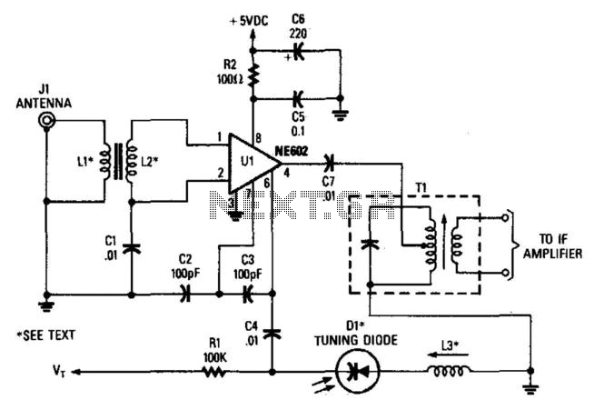
In this configuration, the NE602 serves as a frequency converter in a superheterodyne front-end setup. L1 and L2 form a broadband toroidal transformer, although a tuned transformer may also be utilized. The supply voltage ranges from +5 to +9...
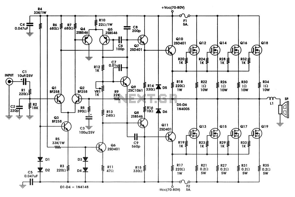
400 W MOSFET Audio Amplifier circuit using IRFP448. This circuit is categorized under amplifiers and includes five circuit diagrams. For more detailed information, refer to the main post titled "400 W MOSFET Audio Amplifier Using IRFP448." This post also...
At 9 volts, the maximum stalled current of the motor types intended for use will be 700 mA. The selection of appropriate MOSFETs is crucial, particularly regarding their ratings for current and voltage handling. However, there are concerns about...
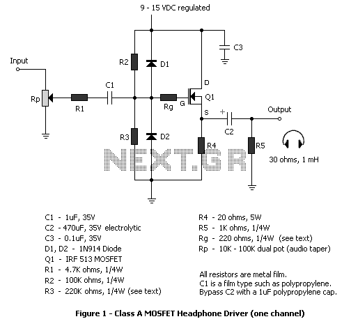
The circuit described in this article is a MOSFET follower for driving headphones. FET followers can supply high current, but have a voltage gain of slightly less than unity. They are most suitable in applications where the input signal...
The supply voltage rails were conservatively maintained at +40V and -40V. For those interested in experimentation, the supply voltage can be increased to a maximum of +50V and -50V, enabling the amplifier to reach its target output of 100W...
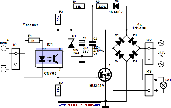
This circuit demonstrates that dimmers designed for mains voltage do not necessarily require a triac. Instead, a MOSFET (BUZ41A, 500 V/4.5 A) is utilized within a diode bridge to manage the voltage across an incandescent bulb using pulse-width modulation...