
Dual limit comparator

The described circuit functions as a voltage comparator with hysteresis, featuring an operational amplifier (op-amp) configuration. When the input voltage surpasses the defined threshold of 8 volts, the op-amp outputs a positive voltage. This behavior is crucial for applications requiring a clear distinction between high and low voltage levels.
The resistors R1, R2, and R3 play a vital role in setting the reference voltages for the op-amp. Specifically, R1 is connected to the inverting input, while R2 and R3 are configured to establish the non-inverting input reference. The ratio of R1 to R2 determines the upper threshold for the positive output, while the ratio of R1 to R3 sets the lower threshold for the negative output. It is essential to ensure that these resistors are selected appropriately to achieve the desired voltage levels.
The forward voltage drop across the diodes in the circuit must be accounted for, as it can affect the accuracy of the output voltage. Diodes typically exhibit a forward voltage drop of approximately 0.7 volts for silicon diodes, which should be included in the calculations when determining the exact threshold voltages.
Inverting the output can be easily accomplished by reversing the inputs to the op-amp. This feature adds versatility to the circuit, allowing it to be used in various applications where an inverted output signal is required.
The use of the 709 operational amplifier without frequency compensation indicates that the circuit is designed for low-frequency applications, where phase margin and stability are less of a concern. However, it is important to consider the bandwidth and slew rate limitations of the 709 to ensure that the circuit performs adequately for the intended application. Overall, this circuit design is efficient for voltage detection and can be adapted for various electronic systems requiring precise voltage thresholds.This circuit gives a positive output when the input voltage exceeds 8 volts. Between these limits the output is negative. The positive limit point is determined by the ratio of Rl, R2, and the negative point by Rl, R3. The forward voltage drop across the diodes must be allowed for. The output may be inverted by reversing the inputs to the op amp The 709 is used without frequency compensation.
Related Circuits
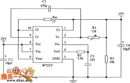
The application circuit depicted below features an output voltage that exceeds the referenced voltage. It utilizes the W723 multi-port adjustable positive voltage regulator, which incorporates current limiting protection. The output voltage can be adjusted within a range of 7V...
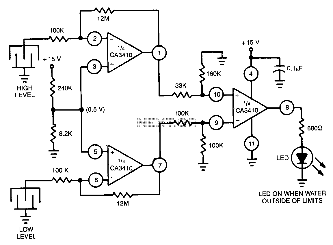
Utilizes the CA3410 quad BiMOS operational amplifier to detect small currents. Due to the low input current of the op-amp, a current as small as 1 pA flowing through the sensor will cause the converter's output to vary by...

Lamp LI will glow brightly while the LED remains off when the battery is low and charging. Conversely, the LED will illuminate brightly, and the light bulb will be dim when the battery is nearly charged. Lamp LI should...
This circuit lights up ten bulbs sequentially, first in one direction and then in the opposite direction, creating an appealing visual effect. In this circuit, gates N1 and N2 form an oscillator. The output of this oscillator serves as...
A video amplifier output arrives at a differentiation stage before the Schottky comparator. The typical propagation delay is reduced to 10 ns. The output pulse width is determined by the capacitance value, where C is 100 pF, resulting in...
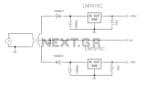
The 7815 regulates the positive supply, while the 7915 regulates the negative supply. The transformer should have a primary rating of 240/220 volts for Europe or 120 volts for North America. The center-tapped secondary coil should be rated approximately...