
DVI-300/2000 Load Step Response

The Dual Voltage/Current Source (DVI) setup described involves a sophisticated circuit design aimed at examining the dynamic behavior of load currents in relation to voltage inputs. The DVI operates under two specified voltage levels, +3V and +5V, which serve as the power supply for the load testing. The incorporation of the NDP7060 n-channel FET allows for effective switching capabilities, where the FET acts as a controlled resistor that can be turned on or off based on the gate voltage.
The switching mechanism is crucial for testing the load current, as it enables the introduction of varying resistances into the circuit. The FET's performance is dictated by its gate-source voltage, which must exceed 2 V to ensure proper operation. This threshold is critical in determining the FET's conductive state and influences the overall performance of the DVI.
The addition of a bypass capacitor serves to stabilize the voltage across the load resistors, minimizing the impact of voltage glitches that occur during rapid changes in load current. This is particularly important in applications where precise voltage control is necessary. The capacitor's role in reducing amplitude while maintaining a steady state is vital for ensuring reliable operation of the DVI.
The use of test configurations across different DVI boards, specifically comparing the DVI-300 and DVI-2000 models, highlights the importance of switching speed and responsiveness in circuit design. The observed differences in glitch amplitudes and areas suggest that careful consideration must be given to the selection of components and their operational parameters to achieve the desired performance.
The testing methodology employed, including the use of an oscilloscope with an AC-coupled probe, allows for detailed analysis of the circuit's behavior under varying conditions. The results indicate that input power levels and load current configurations significantly influence glitch characteristics, thus providing valuable insights into the design and optimization of voltage/current sources in electronic applications. Overall, the findings underscore the complexity of load dynamics in electronic circuits and the necessity for precise engineering to mitigate adverse effects during operation.Channel 0 of the Dual Voltage/Current Source (DVI) was used as the input. Input levels of +3V and +5V were used. Load current was the variable of interest we wanted to relate to the performance of the DVI. One DVI with a maximum of 300 mA and another with a maximum of 2000 mA were tested. The NDP7060 n-channel FET was used to switch in the low res istor, and thus introduced high load current. When the gate voltage is sufficiently greater than the source voltage (minimum of 2 V as specified on the data sheet), the FET turns on and allows current to flow from the drain to the source. Intuitively, when the FET is off, no current is allowed to flow, and so the DVI only sees the high resistance, equivalent to having low current load.
An external driver operated by a switch relay was used to turn the gate on and off. With load resistance and current changing, a voltage glitch of a given amplitude is expected. To minimize the effect of the glitch, the circuit is rewired to include a bypass capacitor attached in parallel with the load resistors. VisualATE and an ASL1000 were used to operate the DVI on slot 9. A simple C+ script was written to operate the channel and external driver to change the load resistance and current.
Glitches were examined at instances were load current changed from low to high and high to low using an AC coupled probe on an oscilloscope. Tests were performed on both DVI boards with and without the bypass capacitor on two load current combinations.
Voltage levels of +3V and +5V were used on the DVI-300 board to test input power effects. In the no capacitor tests, A and C along with E and G were given the same testing parameters of load current on different DVI boards, but the results turned out significantly different. The DVI-2000 board had glitches of smaller peak-to-peak amplitude and lower glitch area. A possible explanation for this is the DVI-2000 having a faster switching responsiveness than the DVI-300, allowing the former less time to experience the effect of load current changes.
This effect was only examined on the DVI-300. It is likely that the DVI-2000 will have the same effect. Looking at test pairs A and B, and pairs E and F, a higher input power level produced higher glitch amplitudes and larger glitch areas. The DVI-300 seems to have a greater amplitude change due to a lowG high load current change than a highG low load current.
Test pairs C/D and G/H show that the larger load currents produced higher glitch amplitude and areas for highG low. However, lowG tests showed that while glitch amplitudes were still higher for higher load currents, glitch areas were lower.
The glitches were quite different depending on the type of load current switch. Overall, glitch amplitudes were significantly larger for highG low change in load current. The glitch area figures seem to be mixed, higher for one load current change with given current settings and lower for the other. The capacitor served its purpose to a slight degree in reducing the effect due to the change in load current by minimizing the amplitude and bringing the system back to steady state quickly.
The amplitudes dropped with the capacitors in all the tests, but the glitch area remained fairly constant. This implies that it took more time for the system to return to its steady state value, and was evident with the oscillations that occurred (see APPENDIX under capacitor tests).
Two different valued capacitors were used, and results showed that the larger one significantly reduced the amplitude, but seemed to increase the glitch by a tiny amount. 🔗 External reference
Related Circuits
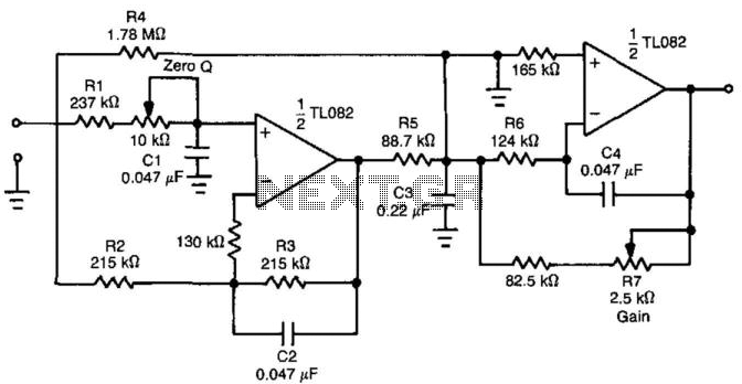
By introducing an additional transmission zero to the stopband of a low-pass filter, a sharper roll-off characteristic can be achieved. The filter design example illustrated in Figure 30-1(a) demonstrates that the time-domain performance of the low-pass section can also...
The circuit depicted can be utilized to control a unipolar stepper motor equipped with four coils. This design is derived from an older fax machine. The circuit is capable of handling a motor current of approximately 500 mA per...
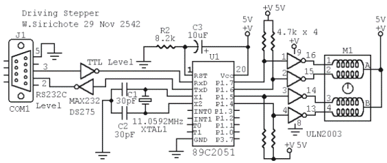
M1 is a stepper motor salvaged from an old disk drive. It features five pins: common, coil 1, coil 2, coil 3, and coil 4. The resistance measured between the common pin and each coil is approximately 75 Ohms....
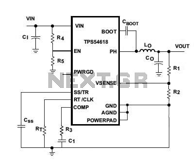
Texas Instruments introduced the TPS54618, a 6-A step-down SWIFT DC/DC converter. The new TPS54618 is a monolithic synchronous switcher featuring two integrated 12-milliohm MOSFETs. The TPS54618 is designed to provide high efficiency and compact solutions for powering a variety of...

An adjustable 5A step-down switching regulator circuit operating at 5 MHz can effectively address various voltage conversion challenges. This circuit utilizes the ST1S03 step-down DC-DC converter, which is also suitable for powering low-voltage digital cores in hard disk drive...
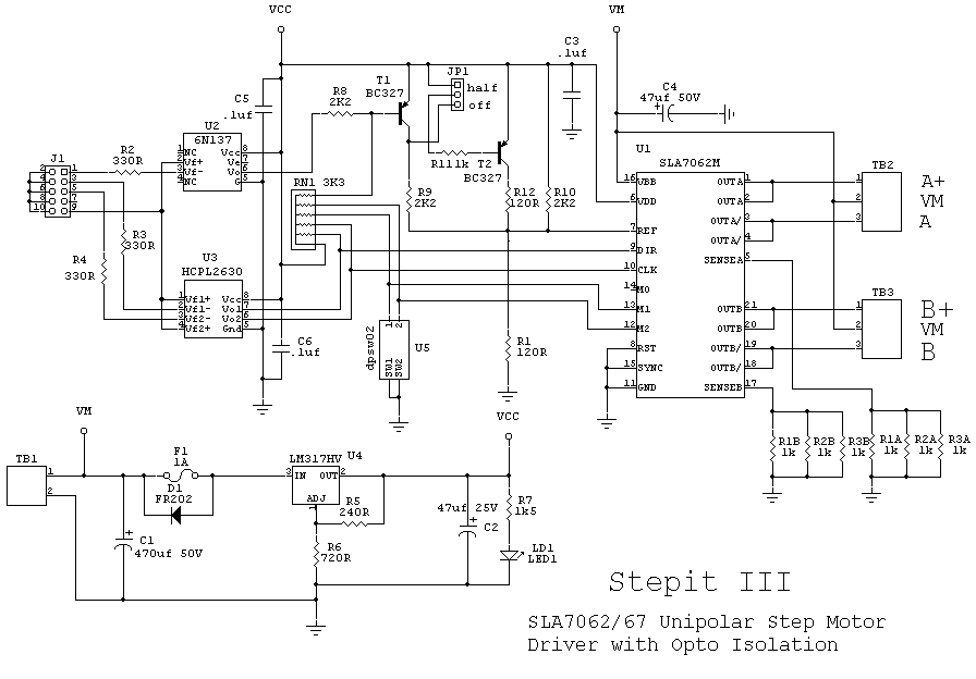
The SLA7062/67 chip is a unipolar driver capable of delivering up to 3 amps. This chip is somewhat difficult to locate and is priced at approximately $10 each. Availability was confirmed through a Google search, which yielded three units...