
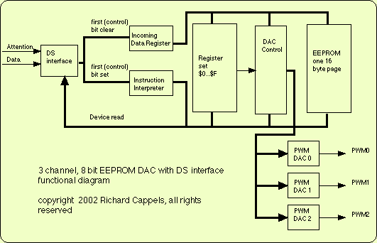
EEPROM DAC with DS interface
With the values for the RC (resistor-capacitor) filters given on the schematic above, the worst-case ripple will be about 1/2 lsb at 5V. Lower power supply voltages cause the ATtiny12's oscillator frequency to drop, thus to maintain 1/2 lsb ripple, it would be necessary to increase the resistors or the capacitors in the output filter.
If during reset initialization, the EEPROM checksum is found to be correct, the DAC values stored in EEPROM will be loaded into the DACs. As such, the DS interface pins can be permanently tied to ground if the situation calls for it. Similarly, if the reset input is not used, the 100k resistor may be omitted and pin 1 tied directly to VCC. If the reset input is tied directly to VCC, check the final assembly language code carefully to make sure that DDRB bit 5 is never set as an output and PB5 is never driven low because port B bit 5 is an alternative function of pin 1.
The DS DAC is composed of a DS interface followed by an Incoming Data Register and an Instruction Interpreter. The instruction interpreter moves to and from the register file and the EEPROM and controls the DAC control. Instructions provide for reading from and writing the register set and the EEPROM.
Using the DS interface, DAC values are written to registers 0, 1, and 2 to control DAC 0, 1, and 2, respectively. The DAC control block creates a bit-reversed image for use by the PWM routines and places them in registers 4, 5, and 6. A command allows the register set and a checksum to be written to a dedicated section of the EEPROM. As part of the reset initialization routine, the EEPROM data are checked against the checksum and if the checksum is valid, registers 0, 1, and 2 will be loaded from the EEPROM and DAC operation commenced using the stored data.
The DS protocol was designed to provide firmware-based bidirectional host-to-slave inter-processor communications for situations in which no hardware solution is available and the host and/or the slave is incapable of tending the interface in real-time. The only specialized hardware required is two bidirectional I/O ports on each chip (alternatively two input ports and two output ports that can be put into a high impedance state may be used).
Sixteen bytes of on-chip EEPROM are accessible directly and usable at the discretion of the programmer. The EEPROM is written every time an instruction to write to the EEPROM (instruction $4X) is interpreted. Since the manufacturer only guarantees the EEPROM to work for a limited number of erase-write cycles (100,000 at the time of this writing), routines that frequently write to the EEPROM should be avoided. Note that when the EEPROM is written, the stored checksum becomes invalid and the automatic loading of the DAC values after reset will not work again until the command to write a new checksum to the EEPROM (command $70) is interpreted.
This DS slave device does not have any internal pull-ups. This chip uses the same PWM generation method as the 8 channel 8 bit DAC.This device provides three channels of 8 bit pulse-width modulation. Output pulse duty cycle ranges from 0 to 255/256 in 255 steps. DACs may be loaded by the DS interface. DAC values may also be copied into the on-chip EERPOM and then automatically be loaded into the DACs when power is applies, making it useful for automatic set up of circuits that do not contain microcontrollers. This replaces more expensive EEPROM DACs and EEPROM pots in many applications, owing to its use of a small area high volume integrated circuit microcontroller.
Additionally, one page of 16 bytes of on-chip EEPROM storage is accessible via the DS interface. With the values for the RC (resistor-capacitor) filters given on the schematic above, the worst case ripple will be about 1/2 lsb at 5V. Lower power supply voltages casue the ATtiny12's osciallator frequency to dorp, thus to maintain 1/2 lsb ripple, it would be necessary to increase the resistors or the capcaitors in the output filter.
If during reset initialization, the EEPROM checksum is found to be correct, the DAC values stored in EEPROM will be loaded into the DACs. As such, the DS interface pins can be permanently tied to ground if the situation calls for it. Similarly, if the reset input is not used, the 100k resistor may be omitted and pin 1 tied directly to VCC.
If the reset input is tied directly to VCC check the final assembly language code carefully to make sure that DDRB bit 5 is never set as an output and PB5 is never driven low because port B bit 5 is an alternative function of pin 1. The DS DAC is composed of a DS interface followed by an Incoming Data Register and an Instruction Interpreter.
The instruction interpreter moves to and from the register file and the EEPROM and controls the DAC control. Instructions provide for reading from and writing the register set and the EEPROM. Using the DS interface, DAC values are written to registers 0, 1, and 2 to control DAC 0, 1, and 2, respectively.
The DAC control blocks creates a bit-reversed image for use by the PWM routines and places them in registers 4,5, and 6. A command allows the register set and a checksum to be written to a dedicated section of the EEPROM. As part of the rest initialization routine, the EEPROM data are checked against the checksum and if the checksum is valid, registers 0,1, and 2 will be loaded from the EEPROM and DAC operation commenced using the stored data.
The DS protocol was designed to provide firmware-based bidirectional host-to-slave inter processor communications for situations in which no hardware solution is available and the host and/or the slave in incapable of tending the interface in real time. The only specialized hardware required is two bidirectional I/O ports on each chip (alternatively two input ports and two output ports that can be put into an high impedance state may be used).
Sixteen bytes of on-chip EEPROM are accessible directly and useable at the discretion of the programmer. The EEPROM is written every time an instruction to write to the EEPROM (instruction $4X) is interpreted -since the manufacturer only guarantees the EEPROM to work for a limited number of erase-write cycles (100,000 at the time of this writing), routines that frequently write to the EEPROM should be avoided.
Note that when the EEPROM is written, the stored checksum becomes invalid and the automatic loading of the DAC values after reset will not work again until the command to write a new checksum to the EEPROM (command $70) is interpreted. This DS slave device does not have any internal pull-ups. This chip uses the same PWM generation method as the 8 channel 8 bit DAC. See this page for details of operation. 🔗 External reference
Related Circuits
This is an outdated version; refer to the latest version on the documentation wiki. If you have one of Hack a Day's Bus Pirates, what should you do with it? Explore 1-Wire, I2C, and SPI EEPROMs using the 3EEPROM...
This simple 220V power interface is designed for monitoring electrical equipment and devices using a computer. The interface only detects whether the monitored device is powered on or off. A key feature of this circuit is the galvanic isolation...
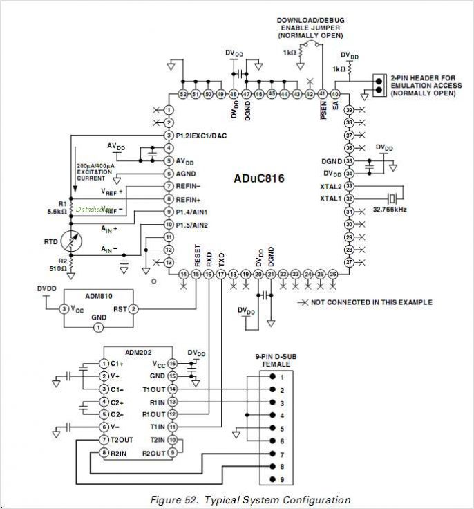
The ADUC831 MicroConverter is a fully integrated 12-bit data acquisition system-on-a-chip. Like all of Analog Devices Inc.'s MicroConverter products, it features precision A/D and D/A conversion along with a Flash Microcontroller on a single chip. The ADUC831 is fully...
Flash memory, also known as flash RAM, is a type of non-volatile semiconductor memory device that retains stored data even when not powered. It is an enhanced version of electrically erasable programmable read-only memory (EEPROM). The primary distinction between...
An LCD (liquid crystal display) is an electronically modulated optical device composed of multiple pixels filled with liquid crystals, arranged in front of a light source (backlight) or reflector to generate images in either color or monochrome. The block...
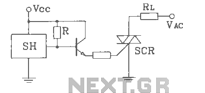
SH Hall opened with a double silicon output interface circuit The SH Hall sensor circuit is designed to provide a dual silicon output interface, which enables enhanced signal processing capabilities. This circuit typically integrates a Hall effect sensor that detects...