
Electronic Coin Toss

The electronic coin toss circuit operates using the CD4049 IC, which is known for its versatility in handling various logic functions. The circuit leverages the properties of the hex inverter to create a simple yet effective coin toss simulator. The relaxation oscillator formed by gates IC1 and IC2 generates a square wave signal, which is essential for providing a random-like output to simulate the unpredictability of a coin toss.
The buffer IC3 plays a crucial role in ensuring that the oscillator's output does not affect the performance of the subsequent stages of the circuit. This isolation is important for maintaining signal integrity, especially when driving loads that may otherwise introduce noise or distortion to the oscillator signal.
The flip-flop configuration using gates IC5 and IC6 allows for a stable output that can indicate the result of the coin toss. When the circuit is activated, one of the LEDs will light up based on the current state of the flip-flop, representing heads or tails. The use of gate IC4 to manage the input logic levels ensures that the flip-flop only toggles its state when appropriate transitions occur, thus preventing false triggering and ensuring reliable operation.
Overall, this coin toss circuit exemplifies a practical application of digital electronics, showcasing how basic components can be combined to create a functional and entertaining device. The design is straightforward, making it an excellent project for those looking to enhance their understanding of digital logic and circuit design.This is electronic coin toss circuit using one CD4049 IC (Hex inverting buffer and TTL driver). This IC has six buffers and it may be used independently. The buffers may be used as simple inverters, as voltage translators, or as current drivers for interfacing TTL or other logic. The gate IC1 and IC2 of the IC and resistor condenser network from a relaxation oscillator. Gate IC3 of the IC is a buffer which isolates the oscillator from the load. Gates IC5 and IC6 are wired as a flip-flop. The LEDs will glow (either head or tail) when the corresponding gate`s output is high. The output of flip-flop will change states only when the input applied are compliment logic levels, example: high and low. For this gate IC4 is used. We aim to transmit more information by carrying articles. Please send us an E-mail to wanghuali@hqew. net within 15 days if we are involved in the problems of article content, copyright or other problems.
We will delete it soon. 🔗 External reference
Related Circuits
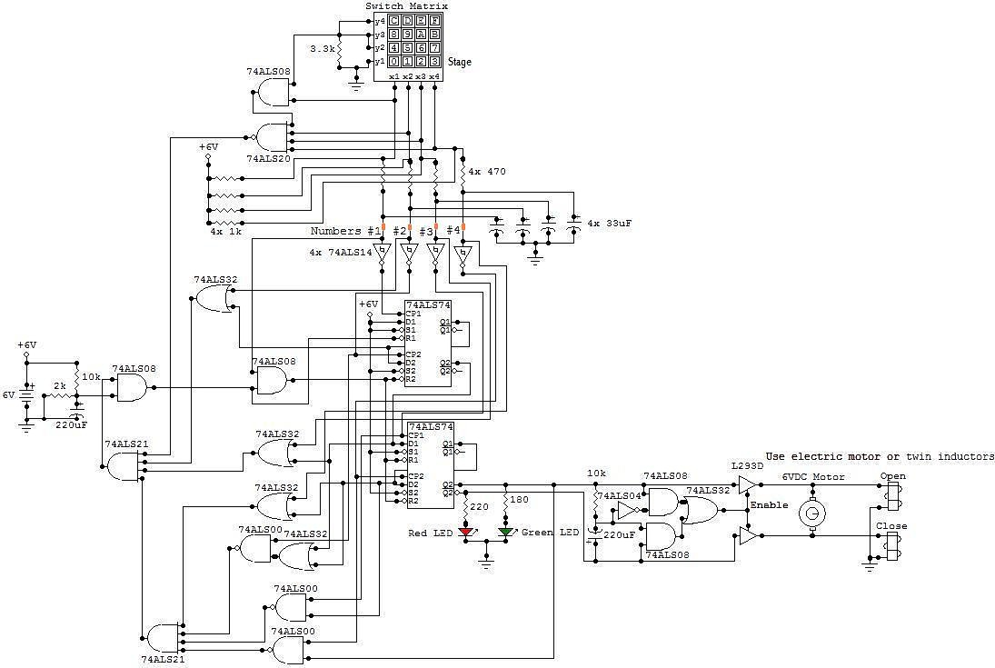
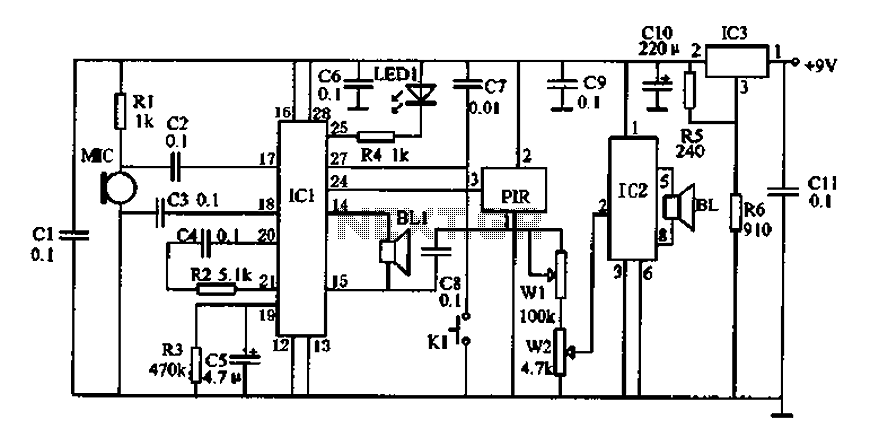
This circuit is an electronic locker that operates using a combination of switches, functioning based on a specific code. The switch matrix is located on the locker door and consists of 16 switches arranged in a 4x4 grid, totaling...
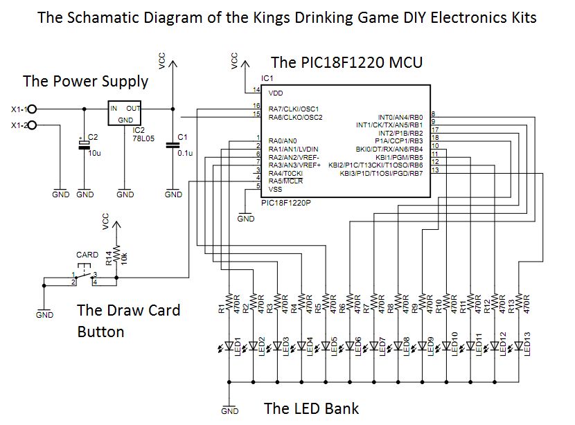
This circuit was designed approximately four months ago and has been developed into a kit for others to use. The circuit in question appears to be a well-thought-out design that has been packaged into a kit format, making it accessible...
This antenna selector circuit diagram electronic project is constructed using standard electronic components and facilitates the switching between two FM antennas through a logic signal. The gates IC1b and IC1a manage the switching and interface between the required logic...
The construction of buildings, when full power is not required, utilizes dimmable electronic ballasts for continuous fluorescent operation, which can further reduce power consumption. Most modern designs and research on electronic ballasts recommend using resonant converter power circuits to...

The TEA5551T monolithic integrated radio circuit can be utilized to design an AM radio receiver circuit intended for portable use with headphones. This circuit incorporates all necessary components for a complete AM radio receiver, including a fully integrated AM...
Doppler effect sensor N1 (RD627), operational amplifier N2 (LM358), and a special integrated circuit for imitating dog barking (N3, KD5608) are utilized along with other components. When there is no activity detected in the monitoring area by N1, the...