
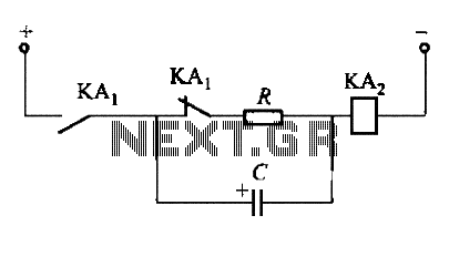
Antenna selector circuit diagram electronic project
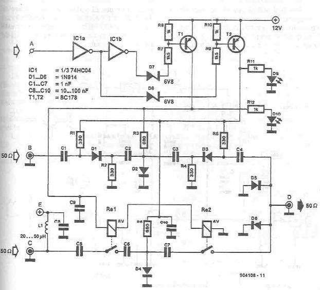
This antenna selector circuit employs a straightforward design that leverages common electronic components to enable effective antenna switching. The circuit utilizes two integrated circuit gates (IC1a and IC1b) to control the logic states required for the operation of the relays, which are responsible for selecting the desired antenna. The logic signals dictate the flow of current through the circuit, ensuring the appropriate relay is activated based on the input state.
In the high logic state of input A, the circuit is designed to route power through T2, which is a transistor that acts as a switch. When activated, T2 allows current to flow through R9 and D8, illuminating D9, which serves as an indicator that the first antenna is selected. This configuration ensures that the first relay (RE1) is energized, allowing the signal from the first FM antenna to pass through to the output.
In contrast, when input A is in a low logic state, the circuit activates T1 instead. This transistor's activation occurs through the pathway of Q1, R7, and D7, which also serves as an indicator by lighting D10. The activation of T1 energizes the second relay (RE2), allowing the second FM antenna to connect to the output. The series configuration of the relays ensures that only one antenna can be selected at a time, preventing signal interference.
The circuit is powered by a dual voltage supply, with 5V and 12V levels necessary for the operation of the logic gates and transistors, respectively. The careful design of the circuit ensures that it can operate reliably in a variety of conditions, making it suitable for applications where antenna selection is needed without manual intervention. The use of common components also facilitates easy assembly and repair, enhancing the practicality of the project for hobbyists and professionals alike.This antenna selector circuit diagram electronic project is designed using common electronic components and allows switching between two FM antennas via a logic signal. Gates IC1b and IC1a provide switching and interface between the logical form of 5 and 12 V supply voltage, required for selection.
When input A is logic state H, IC1a`s output will be L and that of IC1b will be H. In this case, current will flow from the positive supply terminal to IC1a, through T2 R9 and D8; T2 lead and D9 light. When input A is logic state L, then IC1b is L, the current flow from source to IC1b positive connector, through Q1, R7 and D7, then T1 is open and D10 light.
Meanwhile, the two relays connected in series, RE1 and RE2, are placed under voltage, their contacts close and VHF signal appear at C input and D output 🔗 External reference
Related Circuits
The diagram illustrates a straightforward and efficient receiver designed for activating garage doors, starter motors, alarms, warning systems, and various other applications. The silicon-controlled rectifier (SCR) utilized in this circuit features an exceptionally low trigger current of 30 µA,...
In night photography, long exposures are common, sometimes lasting several seconds to several minutes. HDR techniques often require taking a series of nine or more photos. Holding a remote trigger for an extended period can be tedious, leading to...
The industrial fuel oil furnace controller circuit consists of a power supply circuit, a testing and ignition control circuit, and a control implementation circuit, as illustrated in the accompanying diagram. The power supply circuit includes a step-down capacitor (C6),...
To fulfill the requirements of a control loop, it is often necessary to utilize an electromagnetic relay or a transistor relay to either accelerate or delay an action, thereby forming an acceleration or delay circuit. The circuit depicted in...
This example describes a wireless remote control switch featuring reliable operation and practical characteristics, capable of remotely controlling a 6-channel device within a 6-meter range for household electricity. The wireless remote control switch circuit consists of a wireless transmitter...
The LED current drive is regulated and programmable, which eliminates the need for current-limiting resistors. The integrated circuit (IC) features an adjustable voltage reference and an accurate ten-step voltage divider. The LED current drive circuit is designed to provide precise...
Warning: include(partials/cookie-banner.php): Failed to open stream: Permission denied in /var/www/html/nextgr/view-circuit.php on line 713
Warning: include(): Failed opening 'partials/cookie-banner.php' for inclusion (include_path='.:/usr/share/php') in /var/www/html/nextgr/view-circuit.php on line 713