
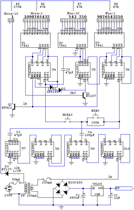
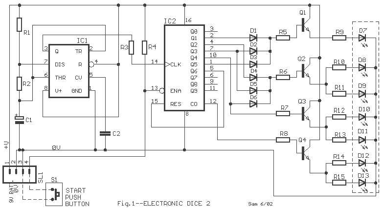
electronic dice
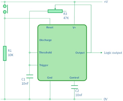
The 555 timer in the astable configuration operates by continuously charging and discharging capacitor C1, resulting in a square wave output. The frequency of oscillation is primarily influenced by the values of C1 and R3, which can be adjusted to achieve the desired tone frequency. This output is fed into the clock input of the 4510B counter, allowing it to increment or decrement its count based on the clock signal's state.
The 4510B counter is designed to handle binary-coded decimal (BCD) outputs, making it suitable for applications such as digital displays. The counter's ability to count both up and down provides versatility in various applications, including games or timers where countdown functionality is essential. The Terminal Count output serves as a crucial feature, allowing for cascading multiple counters in a system, enhancing the overall counting capability.
In applications requiring specific reloading of the counter, the Parallel Load function becomes vital. By setting the PL pin high, the counter can be loaded with a predetermined value, enabling quick resets or adjustments in counting. The interaction between the PL and TC pins, necessitating the use of an NPN transistor for signal inversion, exemplifies the need for careful circuit design to ensure compatibility between different logic levels.
Overall, the combination of the 555 timer and the 4510B counter in this circuit provides a robust solution for generating tones and managing numerical displays, with flexibility in counting direction and reloading capabilities.The 555 astable board uses a 555 timer in its astable configuration. This means that it outputs a square wave or a series of high and low signals. The speed that the signal goes high and low is set by the capacitor C1 and variable resistor R3. The board is designed to make a tone so will be switching quickly on and off which is just what`s require d for the 7 segment dice. The purpose of the 555 timer is to generate a clock signal whenever the switch is pressed. When this happens the 7 segment will be clocked through the various numbers. The circuit diagram of the 555 astable circuit is shown below: The counter selected is a binary coded decimal four bit up down counter (4510B). This means that it can either count up from zero to nine or down from 9 to 0 and that the output of this is indicated in binary.
The diagram above shows how the counter operates when clocked, the solid line indicating a clock when set to up and the dotted line shows the step when clocked in the down mode. The second number in each of the boxes is the binary representation of the data that will be present on the counter outputs Q3 to Q0.
The chip has a Terminal Count (TC) output, this is normally present to allow one counter to trigger another counter when the count wraps around. This pin can however be used to reset the counter itself. The pin is active low so will be low: if counting up - when it reaches nine or if counting down when it reaches zero.
The chip also has a Parallel Load (PL) function. When the PL pin is taken high the data on the inputs P3 to P0 are loaded into the counter. This functionality can be used to reload the counter with any value. So it is possible to load six and count down. When zero is reached the TC pin will change from high to low and this can be used to reload the counter to six. Unfortunately the PL pin is active high and the TC pin is active low, so they can`t be connected directly.
Instead an NPN transistor and pull up resistor need to be used to invert the signal. 🔗 External reference
Related Circuits
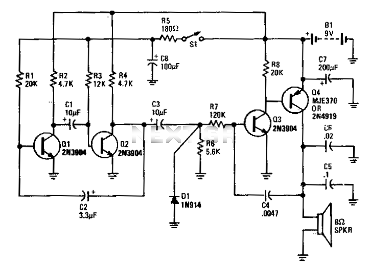
Transistors Q1 and Q2 form the two halves of a free-running multivibrator, with the frequency determined by the voltage across capacitor C8. This capacitor is charged and discharged by the operation of switch S1. Transistors Q3 and Q4 constitute...
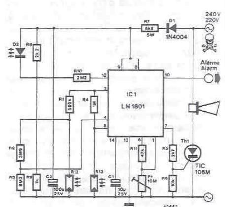
This smoke detector electronic project is designed using the LM1801 and common electronic components. The smoke detector circuit diagram does not utilize ionization detection, gas sensors, or optocouplers; instead, it employs two photoresistors (LDRs) and an LED. The circuit...
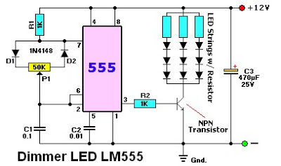
The LM555 timer IC can be utilized in various electronic projects, including the creation of an analog timer. According to the datasheet, the LM555 is versatile and can be adjusted to set timers based on specific requirements. The schematic...
A clock utilizing numeric neon lamps, commonly referred to as nixies. These display devices were prevalent during the 1960s and 1970s, but their usage declined with the advent of LED displays. Today, nixies have become sought-after collectibles and are...
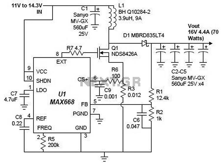
A simple 16-volt switching power supply circuit can be constructed using the provided diagram, which is based on the MAX668 constant-frequency, pulse-width modulating (PWM), current-mode DC-DC controller. This integrated circuit is designed for a wide range of DC-DC conversion...
The IC1 is a 555 timer IC connected for astable operation. The clock pulses are fed to the IC2 via the 10K resistor. The IC2 is a 10-stage counter; output 6 (pin 5) is connected to RESET (pin 15),...