
Electronic Ignition
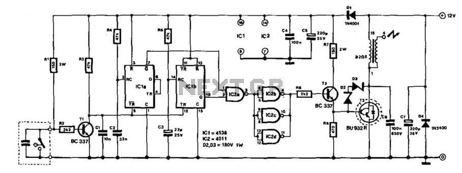
This electronic ignition circuit provides a robust solution for enhancing the efficiency of a conventional car ignition system. By replacing the standard 12-V circuit with a high-voltage system, the ignition process is optimized, leading to improved engine performance. The use of transistors and integrated circuits allows for precise control over the ignition timing and minimizes ignition delay, which is crucial for maintaining engine efficiency and responsiveness.
The circuit's design incorporates several critical components that work together seamlessly. The initial pulse from the contact breaker is vital for triggering the ignition sequence. The differentiation stage, utilizing R3 and C1, ensures that the ignition timing is accurate, allowing for immediate response when the contact breaker is activated. The choice of R1 is significant, as it maintains the cleanliness of the contact points, which is essential for reliable operation and longevity of the ignition system.
The monostable multivibrators, IC1A and IC1B, play a crucial role in managing the timing of the ignition pulse. By responding to different edges of the input pulse, these components ensure that the ignition coil is energized at the optimal moment, enhancing combustion efficiency. The output from IC1A, which is carefully timed by R4 and C2, is critical for controlling the high-voltage Darlington transistor T3, ensuring that it is only activated when necessary, thus preventing unnecessary current draw when the engine is not running.
The protective measures integrated into the circuit, such as the zener diodes, are essential for safeguarding sensitive components from voltage spikes, which can occur during operation. Proper thermal management through the use of a heatsink for the Darlington transistor is also a vital consideration, as it ensures the reliability and durability of the ignition system under varying operational conditions.
Overall, this electronic ignition circuit design represents a significant advancement in automotive ignition technology, providing a more efficient and reliable means of igniting the fuel-air mixture within an engine, ultimately contributing to enhanced vehicle performance and reduced emissions. This electronic ignition circuit is intended to be inserted into a car"s conventional ignition system. In effect, it re places the original 12-V switching circuit in the primary winding of the coil by one generating more than 100 V. It thereby converts a current circuit, which is upset by lead and stray resistance, into a voltage circuit that is much more efficient.
The pulses emanating from the contact breaker, shown at the extreme lower left-hand side of the diagram, are applied to transistor T1 and subsequently differentiated by R3/C1. This causes a negligible ignition delay. The current through the contact-breaker points is determined by the value of R1. This value has been chosen to ensure that the points remain clean. Transistor T1 is followed by two monostables, IC1A and IC1B, which are both triggered by the output pulses of Tl.
However, whereas IC1A is triggered by the trailing edge, IC1B is triggered by the leading edge. Monostable IC1A passes a pulse of about 1.5 ms (determined by R4/C2) to NAND gate IC2A. This gate switches off high-voltage Darlington T3 via gates IC2B, IC2C and IC2D, and driver T2, for the duration of the pulse. Gate IC2 ensures that T3 is switched on only when the engine is running, to prevent a current of some amperes flowing through the ignition coil.
As long as pulses emanate from the contact breaker, IC1B is triggered and its Q output remains logic high. The mono time of this stage is about 1 s and is determined by R5/C3. Darlington T3 is switched on via T2 and IC2A through IC2D as long as IC1A does not pass an ignition pulse.
When the engine is not running, the Q output of IC2B goes low after 1 s and this causes T2 and T3 to be switched off. The two series-connected 180-V zener diodes protect the collector of the BU932R against too high of a voltage.
The Darlington must be fitted on a suitable heatsink. 🔗 External reference
Related Circuits
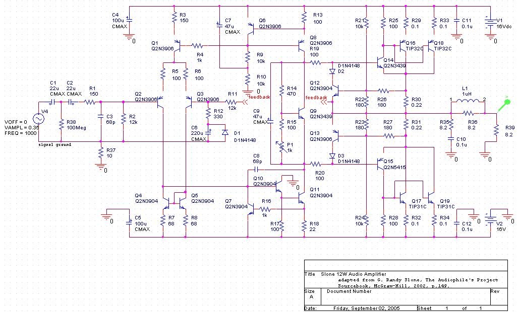
The project involves developing a 12W power amplifier circuit into a fully assembled hard-wired unit. This will require a design cycle and development sequence that includes analysis, simulation, printed circuit board (PCB) layout, board population, hard soldering, and testing....
Modern ICON electronic engine controls from BRP The ICON electronic engine control system developed by Bombardier Recreational Products (BRP) represents a significant advancement in marine technology. This system integrates sophisticated electronic controls to enhance the performance and reliability of marine...
This circuit utilizes a +5 V reference output and an operational amplifier (op amp) to level shift and amplify the 2.1 mV/°C Tempco output into a voltage signal that varies with ambient temperature. Different scaling options can be achieved...
The sphygmomanometer can be categorized into two main types: the mercury sphygmomanometer and the electronic sphygmomanometer. The mercury sphygmomanometer is known for its accuracy, but it requires professional operation and is prone to observational errors due to subjectivity. Additionally,...
The 555 timer IC is connected for Astable Operation, the clock pulses are fed to the 4017 IC via the 10K resistor. The 4017 is a 10 stage counter, output 6 (pin 5) is connected to RESET (pin 15),...
This circuit simulates the dual-tone drone sound produced by an unusual wind instrument. The urjunction transistors Q1 and Q2 are configured in similar audio-oscillator circuits. The frequency of each oscillator is determined by one of the two resistors selected...