
ECE 3434 Electronic Circuits II
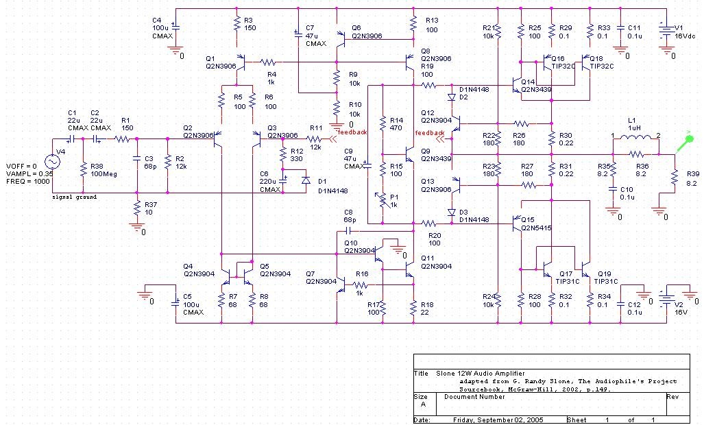
The project focuses on the design and implementation of a 12W power amplifier, which serves as a critical component in various audio applications. The initial phase involves conducting a thorough analysis of the circuit requirements, including determining the specifications for voltage gain, input/output impedance, and frequency response. This analysis will guide the selection of appropriate components, such as transistors, resistors, capacitors, and power supply arrangements.
Following the analysis, simulation of the circuit using PSpice is essential for validating the design before physical implementation. PSpice allows for the modeling of circuit behavior under various conditions, helping to identify potential issues and optimize performance. The simulation results will inform necessary adjustments to component values and configurations to achieve the desired amplifier characteristics.
Once the simulation confirms the design's viability, the next step is the PCB layout. This process involves arranging the components on the board in a manner that minimizes interference and maintains signal integrity. Proper routing of traces is crucial to ensure efficient power distribution and minimize noise.
After finalizing the PCB design, the board will be populated with the selected components. This includes careful placement and soldering, ensuring that all connections are secure and meet quality standards. Hard soldering techniques may be employed to enhance durability and reliability, especially in high-power applications.
Finally, rigorous testing of the assembled unit is essential to verify that the amplifier meets the specified performance criteria. This may involve measuring parameters such as output power, distortion levels, and thermal performance under load conditions. Any deviations from expected results will necessitate further analysis and adjustments to the circuit design or component selection.
Overall, this project encompasses a comprehensive approach to developing a power amplifier, integrating theoretical knowledge with practical skills in electronics design and implementation.The project will take the circuit for a 12W power amplifier and develop it into a completed hard-wired unit. This process will require a design cycle and development sequence consisting of analysis, simulation, PC board layout, population of the board, hard-soldering, and testing.
If for some reason you do not feel secure with the pspice circuit simulation utility you might take a walk through the tutorials under the link to the online resource textbook: R. Winton, Circuits, Devices, Networks, and Microelectronics. They are slow and patient and will help to get you started and into the pspice features needed for the class circuit simulation exercises.
If you are without pspice you can obtain a copy at pspice(olde) which is a relatively friendly version and will help with the overhead needed to come up to speed on the licensed version used by the lab project. 🔗 External reference
Related Circuits
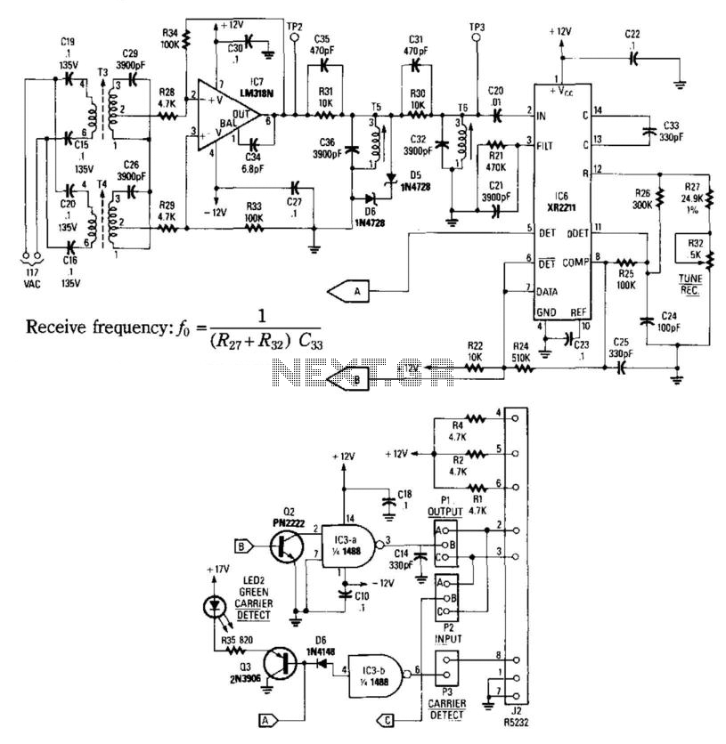
This receiver consists of an input network, amplifier IC7, FSK PLL detector IC8, and output amplifier/interface circuits Q2, Q3, IC3A, and IC3B, which include a 1488 Quad RS232 line driver for the carrier-current signal. The tuned amplifier IC7 amplifies...
The power supply has been simplified. Power transformers and rectifiers have been omitted, and some components from the MOSFET voltage regulator circuits have been removed, including 1N5242 zener diodes between the source and gate and 10k resistors in series...
The construction of buildings, when full power is not required, utilizes dimmable electronic ballasts for continuous fluorescent operation, which can further reduce power consumption. Most modern designs and research on electronic ballasts recommend using resonant converter power circuits to...
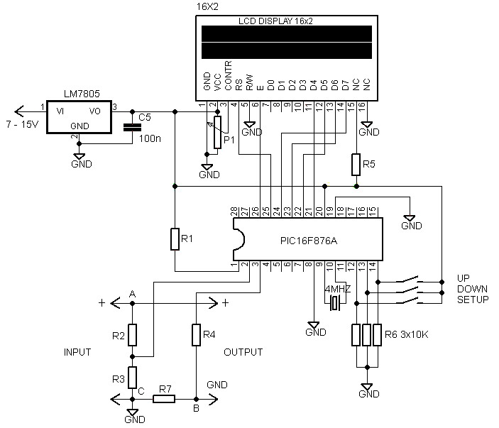
A voltmeter and ammeter using a PIC microcontroller can measure voltage and current simultaneously. This setup employs a PIC16F876A as the data processor for voltage and current measurements. An LCD display (16x2) is utilized to present the measured voltage...
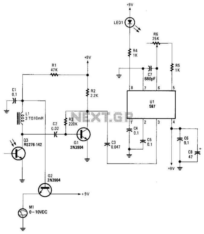
Q3 is an infrared (IR) phototransistor that reacts to a modulated IR beam. Q1 amplifies the alternating current (AC) component of the IR beam. Q2 drives a meter, providing a relative indication of the strength of the light beam,...
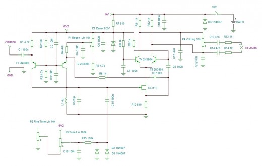
A new high-performance regenerative receiver is available as a kit. The inclusion of an innovative regenerative detector circuit enhances sensitivity and overall performance. The regenerative receiver kit is designed to provide users with a high-quality radio frequency (RF) reception experience....