
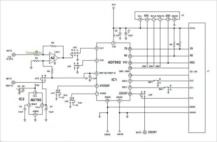
Evaluation Board For Single Supply 12-bit 500 Ksps Adc
The AD9834 evaluation board is designed to facilitate the testing and development of applications using the AD9834 direct digital synthesizer. The board incorporates essential components that enable users to explore the capabilities of the AD9834, which is notable for its ability to generate precise frequency outputs through digital control. The phase accumulator within the AD9834 allows for fine-tuning of the output waveform, while the sine look-up table ensures high fidelity in the generated waveforms.
Operating at clock frequencies of up to 75 MHz, the AD9834 can produce various modulation schemes, including both phase and frequency modulation. This versatility makes it suitable for a wide range of applications in communications and signal processing. The evaluation board connects to a PC's parallel port, providing a straightforward interface for programming and controlling the synthesizer.
Included software simplifies the programming process for the AD9834, allowing users to easily configure output frequencies and modulation parameters. The onboard 75 MHz oscillator generates the necessary master clock (MCLK) for the AD9834, ensuring it operates within its specified performance envelope. However, should the application require different clocking conditions, the onboard oscillator can be bypassed, enabling the connection of alternative clock sources through a BNC connector. This flexibility is advantageous for users who may need to integrate the AD9834 into more complex systems or require specific timing configurations.
Furthermore, the presence of a digital buffer on the evaluation board enhances signal integrity by ensuring that the signals from the edge connector are adequately buffered, minimizing signal degradation and enabling reliable operation. Overall, the AD9834 evaluation board serves as a comprehensive platform for evaluating the performance of the AD9834 DDS, providing users with the tools necessary to develop and optimize their applications effectively.This data sheet describes the evaluation board for the AD9834 direct digital synthesizer (DDS). The AD9834 is a numerically controlled Oscillator using a phase accumulator, a sine look-up table, and a 10-bit DAC The AD9834 CAN be operated with Clock frequencies up to 75 MHz. Both phase modulation and frequency modulation CAN be perfor med with the AD9834. Complete specifications for the AD9834 are available in the AD9834 data sheet and should be consulted in conjunction with this data sheet when using the evaluation board. The evaluation board Interfaces to the parallel port of a PC. Software is available with the evaluation board that allows the user to easily program the AD9834. The AD9834 evaluation board includes a 75 MHz Oscillator that provides the MCLK for the AD9834. The user CAN remove this Oscillator if required, and drive the AD9834 with a different Clock Oscillator or an external Clock source via a BNC connector.
A digital Buffer is also on the board so that the signals from the edge connector are buffered. 🔗 External reference
Related Circuits
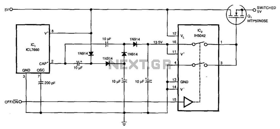
Requiring only 10 µA of quiescent current, the circuit produces an ON-resistance of only 0.1 ohm. IC1 serves as a charge pump voltage converter to generate a 5V level, allowing analog switch IC2 to provide a 10V swing to...

This schematic represents a radio receiver circuit based on the TDA7088T, which is suitable for use in mono portable and pocket radios. The TDA7088T is a bipolar integrated circuit designed to operate with a minimal number of peripheral components...
500 Series immersion temperature probe, NTC, 100,000 Ohm, ±1.5 °C [±2.7 °F] tolerance, 10 °C to 260 °C [50 °F to 500 °F] accuracy, stainless steel, bullet housing, flying leads (two), 26 gauge Teflon insulation, 4,267 mm [168 in]. The...
A voltage divider is created using resistors R2 (10MΩ) and R3 (100KΩ), which effectively reduces the voltage across capacitor C2 by a factor of approximately 100. The ground of C2 is connected to the inverter ground for reference. An...
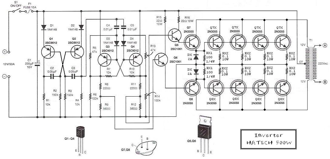
This is the schematic diagram of a 500W power inverter circuit built using 10 pieces of well-known NPN power transistors, 2N3055, to amplify the AC signal produced by a multivibrator. The frequency generator/multivibrator is also constructed using transistors. All...
Universal Power Supply Module 3V-30V power supply. Refer to the specified page for an explanation of the related circuit diagram. This power supply circuit is paired with a high-power audio amplifier rated at 1500 watts. The design of the...