
5V Supply High-Side Switcher
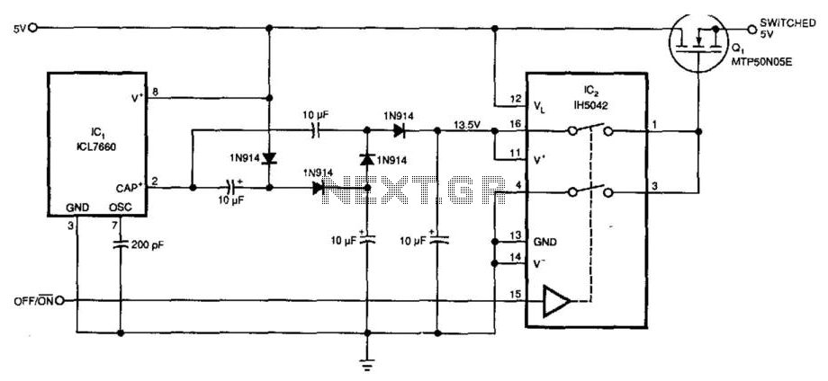
The circuit described operates with a remarkably low quiescent current of 10 µA, making it suitable for applications where power efficiency is critical. The primary component, IC1, functions as a charge pump voltage converter, stepping up the input voltage to a stable 5V. This voltage is essential for the operation of the analog switch IC2, which is responsible for generating a 10V swing necessary for driving the MOSFET Q1.
MOSFET Q1 is a key element in this circuit, acting as a logic level NMOS power transistor. The circuit design allows the analog switch to apply a 4.3V swing to Q1, which is optimized for low ON-resistance, typically around 0.03 ohm. This low resistance is crucial for minimizing power loss during operation, enhancing the efficiency of the overall circuit.
The implementation of additional stages in the voltage-multiplying circuit is a significant feature of this design. These stages increase the gate voltage swing, which is vital for ensuring that the NMOS switching transistor operates effectively. By providing a higher gate voltage, the circuit ensures that the NMOS transistor can switch on and off rapidly, which is essential for high-speed applications.
Overall, this circuit exemplifies a well-engineered design that prioritizes low power consumption and efficient operation, making it suitable for a variety of electronic applications where performance and efficiency are paramount. Requiring only 10uA of quiescent current, the circuit of (Fig. 62-1 (a)) produces only 0.1ohm ON-resis-tance. IC1 is a charge pump voltage converter to produce a 5V level, so analog switch IC2 can provide a 10-V swing to MOSFET Ql. This circuit uses a voltage converter to enable the analog switch to apply a 4.3V swing to logic level NMOS power transistor Q1.
ON resistance is 0.03ohm typical. This circuit uses additional stages in the voltage-multiplying circuit to provide a higher gate voltage swing. This would enable the use of a converter for an NMOS switching transistor. 🔗 External reference
Related Circuits
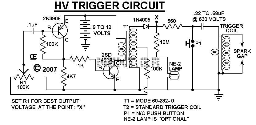
A Very Low Current, High Voltage Spark, that is Manually Triggered. Although its not easily Measured, the Peak Output voltage will be over 5,000 Volts. T1 is a small audio transformer and it steps up the voltage to about...
Rsense will cause Q2 to conduct when a threshold of approximately 0.65V is reached. Rbias will determine the extent of this limitation, although this aspect remains unclear. Particularly, if Rsense is positioned on the high side, simply activating Q2...
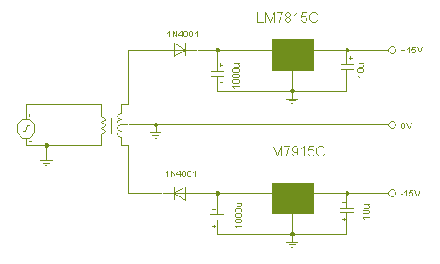
In this circuit, the 7815 regulates the positive supply, and the 7915 regulates the negative supply. The transformer should have a primary rating of 240/220 volts for Europe, or 120 volts for North America. The centre tapped secondary coil...
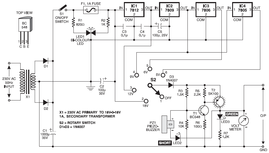
Stabilized DC Power Supply with Short-Circuit Indication. The circuit provides four distinct regulated DC outputs (12V, 9V, 6V, and 5V) along with an unregulated 18V DC output, selectable via a rotary switch S2. The chosen output is displayed on...
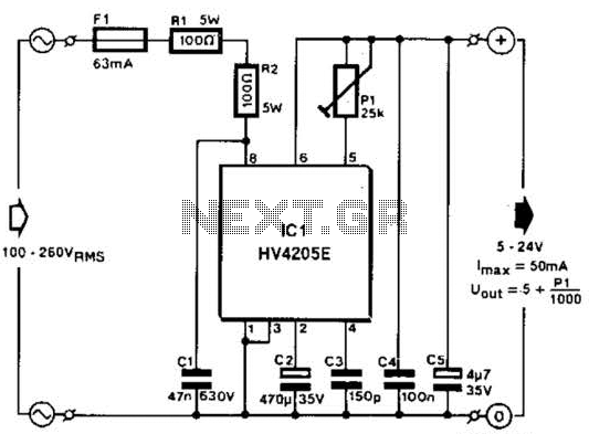
Direct derivation of 5 to 24 Vdc from AC mains without a transformer is possible with this circuit. Note that a direct mains connection to the DC output exists. Suitable safety precautions must be taken. This circuit design allows for...
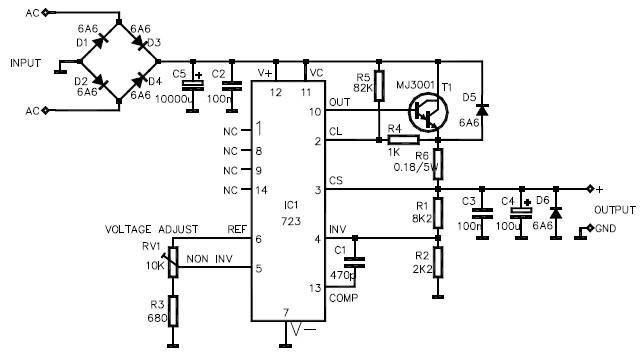
This LM723 variable power supply circuit design is a straightforward variable power supply capable of delivering an output voltage ranging from 8 to 30 volts, with a maximum output current of 3 amperes. The circuit features a low output...