
exponential vf converter for electronic music
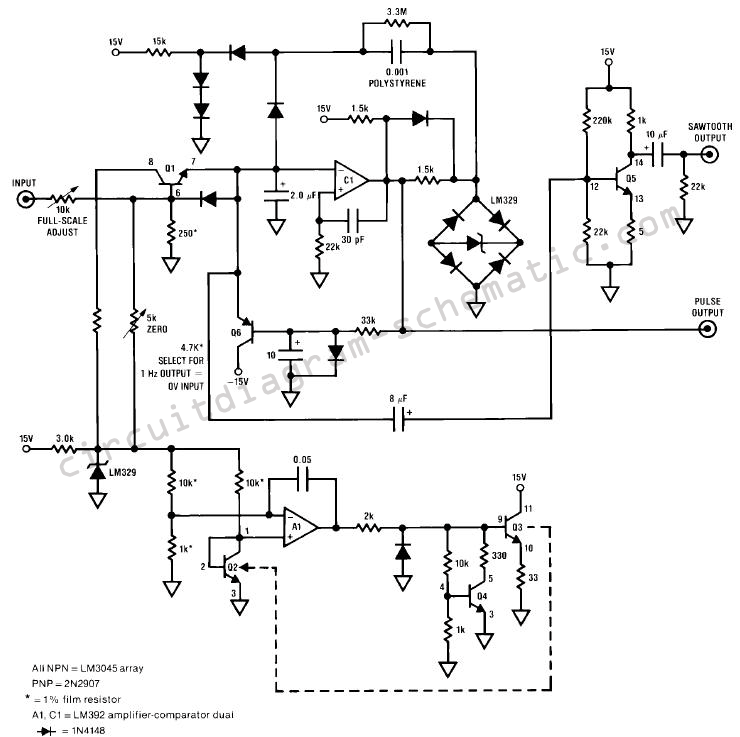
The circuit operates primarily through the interaction of the LM392 and the LM3045 transistor array. The LM392 serves as a comparator, which is essential for monitoring the output state of C1 and controlling the switching of the capacitor. The LM3045 array, which includes multiple transistors, is designed to maintain thermal stability, thus ensuring consistent performance across varying environmental conditions. The use of Q2 and Q3 as a heater-sensor pair is critical; their configuration allows for precise temperature control, which mitigates the effects of thermal drift that can adversely affect the exponential function generated by Q1.
The charge dispensing interface converter is a crucial component that translates the current output from Q1 into a usable signal. The integration of the 0.001 µF capacitor with the reference voltage establishes a timing mechanism that allows for accurate signal processing. The LM329 zener diode bridge provides a stable reference voltage, which is essential for the reliable operation of the circuit.
The regenerative feedback loop formed by the 30 pF capacitor and the 22 kΩ resistor is a key feature that enhances the circuit's performance. This feedback mechanism ensures that the output of C1 is reinforced, leading to improved response times and stability in the circuit's operation. As the feedback loop decays, it allows for a reset of the system, preparing it for the next cycle of operation. Overall, this circuit design exemplifies an effective approach to achieving precise exponential conformity across a specified frequency range while addressing potential thermal issues through careful component selection and configuration.The diagrams a circuit which performs this function with 0. 25% exponential conformity over a range from 20 Hz to 15 kHz using a single LM392 and an LM3045 transistor array. The exponential function is generated by Q1, whose collector current will vary exponentially with its base-emitter voltage in accordance with the well known relationship betwee
n BE voltage and collector current in bipolar transistors. Normally, this transistor`s operating point will vary wildly with temperature and elaborate and expensive compensation is required. Here, Q1 is part of an LM3045 transistor array. Q2 and Q3, located in the array, serve as a heater sensor pair for A1, which servo controls the temperature of Q2.
This causes the entire LM3045 array to be at constant temperature, eliminating thermal drift problems in Q1 ²s operation. Q4 acts as a clamp, preventing servo lock-up during circuit start-up. Q1 ²s current output is fed into the summing junction of a charge dispensing I/F converter. Here is s schematic drawing : C1 ²s output state is used to switch the 0. 001 uF capacitor between a reference voltage and C1 input. The reference voltage is furnished by the LM329 zener diode bridge. The comparator`s output pulse width is unimportant as long as it permits complete charging and discharging of the capacitor.
In operation, C1 drives the 30 pF-22k combination. This RC provides regenerative feedback which reinforces the direction of C1 ²s output. When the 30 pF-22k combination decays, the positive feedback ceases. 🔗 External reference
Related Circuits
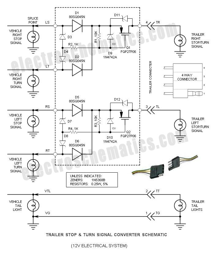
If you have ever wondered why the Stop/Turn signal lamps on your trailer appear dim, you are not alone. The reason for this is that the typical Stop & Turn Signal Converter... The dimming of trailer Stop/Turn signal lamps is...
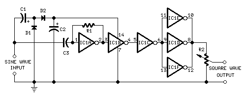
This circuit is intended to provide good square waves converting a sine wave picked up from an existing generator. Its main feature consists in the fact that no power source is needed: thus it can be simply connected between...
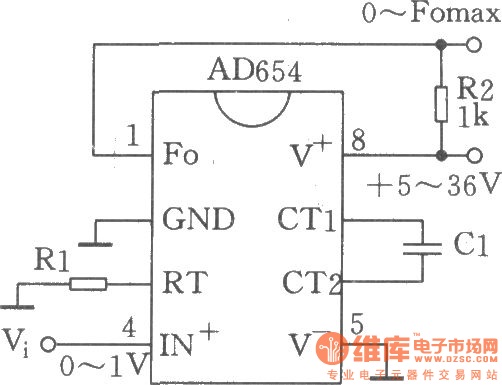
The circuit depicted is a low-cost voltage frequency converter (VFC) utilizing the AD654 component. By connecting the required components, Rl and Cl, as shown in the figure, a functional VFC application circuit can be established. The supply voltage can...
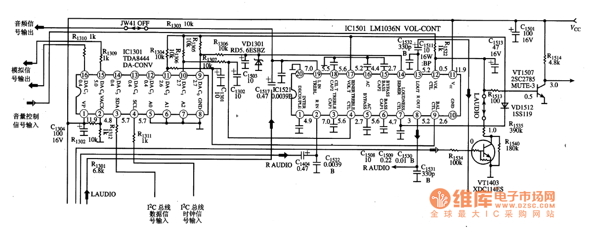
The TDA8444 is a digital-to-analog (D/A) converter integrated circuit (IC) produced by Philips. It is designed to convert digital signals into analog signals. The TDA8444 IC utilizes a 16-pin dual in-line package, with specific pin functions and data outlined...
This circuit is a simple DC to DC converter designed for digital circuits. It operates with a supply voltage of 5V and provides an output voltage that steps up to a maximum of 10V-12V DC. The circuit utilizes an...
This electronic ignition circuit is designed to be integrated into a conventional car ignition system. It replaces the original 12-V switching circuit in the primary winding of the ignition coil with a circuit that generates over 100 V. This...