
Sine to Square wave Converter

The circuit operates by first receiving an input sine wave from a generator, which is typically characterized by a smooth, periodic oscillation. The voltage doubler, consisting of capacitors C1 and C2 along with diodes D1 and D2, is responsible for increasing the voltage level of the incoming sine wave. This voltage doubling is crucial as it provides the necessary power to the integrated circuit (IC) without the need for an external power source, making the circuit highly efficient and portable.
Once the sine wave is processed by the voltage doubler, the amplified signal is fed into the operational amplifier stage, specifically IC1A. This stage enhances the amplitude of the sine wave, ensuring that it reaches a sufficient level for further processing. The operational amplifier is configured to operate in a non-inverting mode, maximizing the output voltage swing.
Following amplification, the signal is routed to a series of inverters integrated within IC1. These inverters are designed to convert the amplified sine wave into a square wave. The squaring process involves toggling the output state each time the input crosses a certain threshold, effectively creating a digital representation of the original sine wave. The output square wave maintains a consistent mark/space ratio, which is essential for applications requiring precise timing and control signals.
The final output is a square wave that can be utilized for various applications, including driving digital circuits, clock signals, or testing equipment that requires a square wave input. The circuit's simplicity and efficiency make it a valuable tool for engineers and technicians working with waveform generation and signal processing.This circuit is intended to provide good square waves converting a sine wave picked-up from an existing generator. Its main feature consists in the fact that no power-source is needed: thus it can be simply connected between a sine wave generator and the device under test.
The input sine wave feeds a voltage doubler formed by C1, C2, D1 & D2 that powers the IC. IC1A amplifies the input sine wave, other inverters included in IC1 squaring the signal and delivering an output square wave of equal mark/space ratio and good r 🔗 External reference
Related Circuits

A step-up converter can be designed using the MAX641 integrated circuit from Maxim IC, utilizing a minimal number of electronic components. This high-voltage step-up converter project can deliver a maximum output current of up to 1A. The low battery...
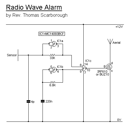
This simple circuit is sure to have the police beating a path to your door - however, it has the added advantage of alerting you to their presence even before their footsteps fall on the doormat. The described circuit functions...
Currently, high-power, high-frequency, narrow pulsing applications primarily utilize vacuum tubes, such as secondary electron transmitting tubes, discharge gap switches, trigatrons, and hydrogen brake pipes. The main research focus is on improving the switching speed of these vacuum devices, aiming...
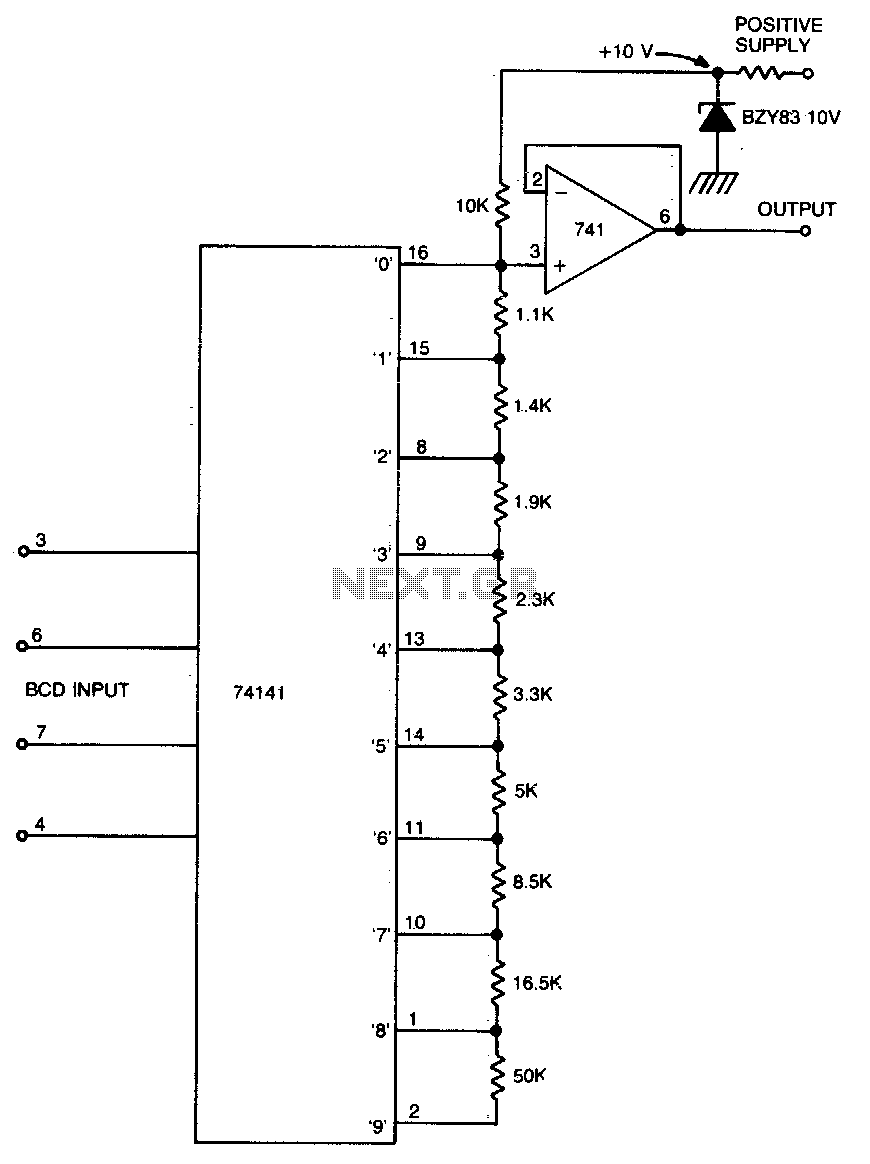
This circuit converts a four-bit Binary-Coded Decimal (BCD) into a variable output voltage ranging from 0 to 9 volts in 1-volt increments. The SN74141 functions as a Nixie tube driver, featuring ten open-collector outputs. These outputs are utilized to...
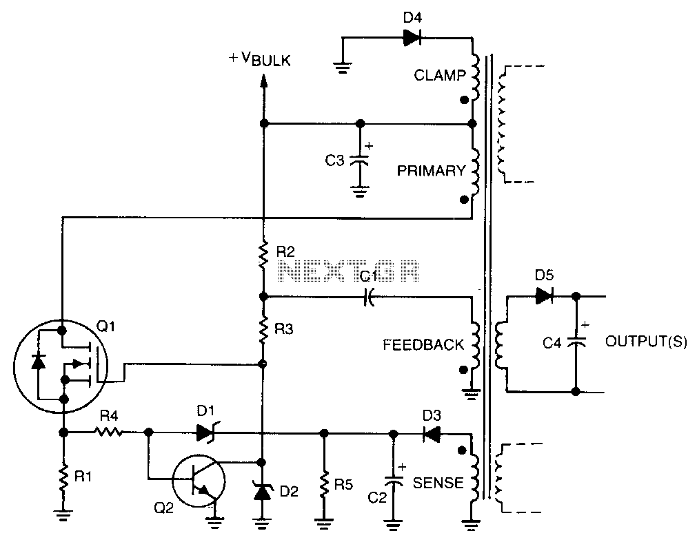
Regulation is achieved by using the rectified output from the sense winding, which is applied as a bias to the base of transistor Q2 through Zener diode D1. The collector of Q2 then disconnects the drive from the gate...
The LT3483/LT3483A are micropower inverting DC/DC converters featuring integrated Schottky diodes and a single resistor feedback mechanism. Their compact package size, high integration level, and the use of small surface mount components allow for a solution size as small...