
Fading LEDs schematic
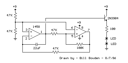
The circuit consists of two operational amplifiers (opamps), one producing a slow rising and falling voltage from about 3 volts to 6 volts, and the other (on the right) is used as a voltage comparator, the output of which supplies an alternating voltage switching between 2 and 7 volts to charge and discharge the capacitor with a constant current.
Each of the op-amps has one of the inputs (pins 3 and 6) tied to a fixed voltage established by two 47K resistors so that the reference is half the supply voltage or 4.5 volts. The left opamp is connected as an inverting amplifier with a capacitor placed between the output (pin 1) and the inverting input (pin 2). The right opamp is connected as a voltage comparator so that the output on pin 7 will be low when the input is below the reference and high when the input is higher than the reference. A 100K resistor is connected between the comparator output and input to provide positive feedback and pulls the input above or below the switching point when the threshold is reached. When the comparator output changes at pin 7, the direction of the current changes through the capacitor which in turn causes the inverting opamp to move in the opposite direction. This yields a linear ramping waveform or triangle waveform at pin 1 of the inverting opamp. It is always moving slowly up or down, so that the voltage on the non-inverting input stays constant at 4.5 volts.
Adjustments to the point where the LEDs extinguish can be made by altering the resistor value at pin 3 and 6 to ground. A 56K in place of the 47K shown worked a little better with the particular LEDs used. Experimentation with this value can yield the desired effect.
Parts List:
Description Mfg Part# Allied Part# Quantity Cost
Operational Amplifier LM1458 288-1090 1 .48
47K Resistor 296-2182 4 .42
100K Resistor 296-5610 1
100 Ohm Resistor 895-0465 1 .24
Transistor 2N3904 568-8253 1 .1
22uF Capacitor 852-6516 1 .07
Solderless Breadboard 237-0015 1 6.99
Red Light Emitting Diode (LED) 670-1224 2 0.50
Note: The LED listed has a narrow viewing angle of 30 degrees and appears brightest when looking directly at it. It's not a pure red color, and a little on the orange side, but should be brighter compared to other selections. For a wider viewing angle at reduced intensity, try part number 670-1257 which is viewable at 60 degrees and has a red diffused lens.
Construction details:
The layout of the solderless breadboard is organized in rows labeled A-J, and columns numbered 1 to 65. Each group of 5 holes in the same column are interconnected, meaning holes A1, B1, C1, D1, and E1 are all connected. The outer rows along the length of the board are also interconnected, typically used for power supply connections. However, there is a break in the mid-section of the outer rows, necessitating the installation of a short jumper wire to connect the entire outer row together. Familiarity with the board layout can be gained by using a digital multimeter (DMM) to probe the various holes.
When installing components, the LM1458 should be oriented with the nook or punch mark near column 30, straddling the center section of the board. Pin 1 of the IC occupies hole E30, while pin 8 is in hole F30. The pins are numbered counterclockwise, placing pin 4 in F33 and pin 5 in E33. Connections for the LM1458, the 9-volt battery, and other components are illustrated in the accompanying schematic diagram.
The installation of components should follow the schematic diagram, ensuring they connect to the appropriate pins of the LM1458. For instance, the 22uF capacitor connects between pins 1 and 2 of the IC, which occupy holes (F30, F31); however, it can be placed in other holes as needed, utilizing jumper wires when necessary for connections across the chip.
The assembled connections include:
- LM1458: F30 to F33, and E30 to E33
- 22uF capacitor: H30 to H31
- 47K resistors: I30 to I35, C27 to C31, F25 to positive battery row, J25 to negative battery row
- 100K resistor: B31 to B33
- 2N3904 Transistor: G36, G37, G38 with emitter at G38
- 100 Ohm resistor: D38 to F38
- LEDs: B43 to B44 (Cathode at B44), I43 to I44 (Cathode at I43)
- Jumper connections for power and signal routing, as detailed in the construction notes
- 9 Volt Battery: Positive battery row to negative row.This circuit is used to slowly illuminate and fade a pair of red LEDs (light emitting diodes). The fading LEDs could be installed as 'eyes' in a small pumpkin or skull as a Halloween attraction, or mounted in a Christmas tree ornament. Or, they might be used as a fancy power indicator for your computer, microwave oven, stereo system, TV, or other appliance.
In operation, a linear 3 volt (peak to peak) ramping waveform is generated at pin 1 of the LM1458 IC and buffered with an emitter follower transistor stage. The 22uF capacitor and 47K resistor connected to pin 2 establish the frequency which is about 0.5 Hz.
You can make the rate adjustable by using a 100K potentiometer in place of the 47K resistor at pin 2. The circuit consists of two operational amplifiers (opamps), one producing a slow rising and falling voltage from about 3 volts to 6 volts, and the other (on the right) is used as a voltage comparator, the output of which supplies a alternating voltage switching between 2 and 7 volts to charge and discharge the capacitor with a constant current.
Each of the op-amps has one of the inputs (pins 3 and 6) tied to a fixed voltage established by two 47K resistors so that the reference is half the supply voltage or 4.5 volts. The left opamp is connected as an inverting amplifier with a capacitor placed between the output (pin 1) and the inverting input (pin 2).
The right opamp is connected as a voltage comparator so that the output on pin 7 will be low when the input is below the reference and high when the input is higher than the reference. A 100K resistor is connected between the comparator output and input to provide positive feedback and pulls the input above or below the switching point when the threshold is reached.
When the comparator output changes at pin 7, the direction of the current changes through the capacitor which in turn causes the inverting opamp to move in the opposite direction. This yields a linear ramping waveform or triangle waveform at pin 1 of the inverting opamp. It is always moving slowly up or down, so that the voltage on the non-inverting input stays constant at 4.5 volts.
Adjustments to the point where the LEDs extinguish can be made by altering the resistor value at pin 3 and 6 to ground. I found a 56K in place of the 47k shown worked a little better with the particular LEDs used. You can experiment with this value to get the desired effect. Parts List: Description Mfg Part# Allied Part# Quantity Cost Operational Amplifier LM1458 288-1090 1 .48 47K Resistor 296-2182 4 .42 100K Resistor 296-5610 1 100 Ohm Resistor 895-0465 1 .24 Transistor 2N3904 568-8253 1 .1 22uF Capacitor 852-6516 1 .07 Solderless Breadboard 237-0015 1 6.99 Red Light Emitting Diode (LED) 670-1224 2 0.50 Note: The LED listed has a narrow viewing angle of 30 degrees and appears brightest when looking directly at it.
It's not a pure red color, and a little on the orange side, but should be brighter compared to other selections. For a wider viewing angle at reduced intensity, try part number 670-1257 which is viewable at 60 degrees and has a red diffused lens.
Construction details: Layout of the solderless breadboard: Refer to the drawing below the schematic diagram and note the solderless breadboard is arranged in rows labeled A-J, and columns numbered 1 to 65. Each group of 5 holes in the same column are the same connection, so that holes A1,B1,C1,D1 and E1 are all connected together.
Likewise holes F1,G1,H1,I1 and J1 are all the same connection. The outer rows along the length of the board are also connected together and are normally used for power supply connections. However, there is a break in the mid section of the outer rows, so a short jumper wire connecting the mid section of the outer rows should be installed to connect the entire outer row together.
If you have a DMM, use the low ohms range and probe the various holes to get familiar with the board layout. Installing the components: Orientate the LM1458 so the nook or punch mark on one edge is near column 30 and the opposite edge is near column 33.
Install the LM1458 on the breadboard so the pins straddle the center section of the board and pin 1 of the IC is occupying hole E30 and pin 8 is in hole F30. The pins are numbered counter clockwise, so pin 4 will be occupying F33 and pin 5 will be in E33. Possible connections for the LM1458, 9 volt battery, and a couple other parts is illustrated in the lower drawing of the solderless breadboard, but it is not complete with all parts.
Refer to the schematic diagram, and install the various other components so they connect to the appropriate pins of the LM1458. Use whatever connection holes are convenient. For example, the 22uF capacitor connects between pins 1 and 2 of the IC, which occupy holes (F30,F31) so it could be placed in the holes (H30, H31) or (J30,J31) or (I30,I31).
But not all parts will conveniently fit, so you may have to use a short jumper wire (#22 preferred) to connect parts from one side of the chip to the other. The board I assembled was connected this way: LM1458 F30 to F33, and E30 to E33 22uF capacitor H30 to H31 47K resistor I30 to I35 47K resistor C27 to C31 47K resistor F25 to Positive battery row 47K resistor J25 to Negative Battery row 100K resistor B31 to B33 2N3904 Transistor G36, G37, G38 with emitter at G38 100 Ohm resistor D38 to F38 LED B43 to B44 (Cathode at B44) LED I43 to I44 (Cathode at I43) Jumper A30 to Positive battery row Jumper F36 to Positive battery row Jumper J33 to Negative battery row Jumper J43 to Negative battery row Jumper H25 to J32 Jumper J30 to J37 Jumper E27 to G31 Jumper D32 to G32 Jumper D33 to H35 Jumper C38 to C43 Jumper E44 to F44 9 Volt Battery Postive battery row to negative row.
🔗 External reference
Related Circuits
Electronic circuits are presented in schematic form. A schematic is essentially a map that illustrates the path of current through various components. Each component is represented by a symbol, typically accompanied by a label or a value, or both....
Electronic Project EPROM Emulator. This EPROM Emulator was designed to complement the EPROM Programmer (Mark 2). The EPROM Emulator serves as a versatile tool for testing and developing electronic circuits that utilize EPROM (Erasable Programmable Read-Only Memory) chips. This device...
The oscillator generates a 1 MHz and a 1 kHz clock signal. The 1 MHz clock serves as the primary clock for the microcontroller and provides a time base for millisecond measurements. A 2 MHz signal is divided by...
This is a straightforward project suitable for individuals with basic electronic skills. Connecting this circuit to an audio source will cause the LEDs to blink in sync with the rhythm. The described project is an audio-activated LED circuit that visually...

A schematic diagram is a layout of symbols and connections representing every electronic component in a circuit, serving as a guide to understanding how the circuit functions. Learning to read these diagrams may initially seem challenging, but it is...
This power supply utilizes a single 7812 IC voltage regulator along with multiple external pass transistors, enabling it to deliver output load currents of up to 30 amps. The circuit design incorporates a 7812 linear voltage regulator, which is...
Warning: include(partials/cookie-banner.php): Failed to open stream: Permission denied in /var/www/html/nextgr/view-circuit.php on line 713
Warning: include(): Failed opening 'partials/cookie-banner.php' for inclusion (include_path='.:/usr/share/php') in /var/www/html/nextgr/view-circuit.php on line 713