
FAST CHARGER controlled by a 68HC11
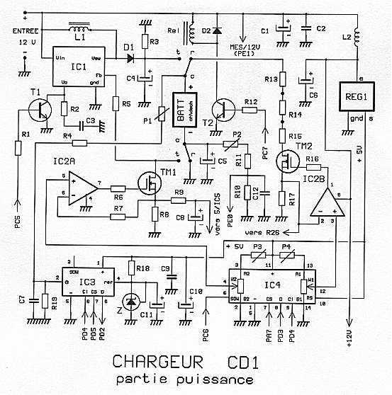
Now note the presence of IC3: this is our precision voltmeter! It is 12 bits, thus capable of 4096 points. We calibrate it to measure from 0 to 40.95 V at 1 / 100 of volts. This converter requires an external reference of 2.5 V. Z is the zener (TL431) which provides. The final calibration is done by P1. In discharge mode, the - batt is grounded by the relay, so the voltage measurement is not a problem.
Circuits IC4 and IC3 are SERIAL programming. So the ?C which will manage the mission of these two circuits. IC3 is a MAX1241 from MAXIM. IC4 is an AD8402 (10 k W ) ANALOG DEVICES. Readers interested in the functioning of these circuits may, as we did, download the files of these circuits on the Web sites of these manufacturers.
Now to the circuit CHARGE. It is located at the top left of the figure. For charging, the relay switches to work. Consider first the case of charging a battery with small number of elements, such as a 4 elements therefore of 4.8 V. Under these conditions, the input of 12V battery is perfectly sufficient for this load. The circuit IC1 is inactive and the current flows through L1, D1 to return to the ground by the constant current generator built with IC2A and TM1. This setup is quite similar to that of discharge, with adjustable intensity and IC4 potentiometer 10 k W. Note that the battery will charge to 5.6 V for charge termination. If an estimated loss of 1 V voltage in L1 and D1, it develops a voltage of 12 to 1 - 5.4 = 5.6 V between drain and TM1 mass. This voltage is fed to the input FB (feedback) of IC1 and as this voltage exceeds 1.25 V, this circuit is blocked.
Now imagine a battery of 12 elements is about 18 V charge termination. This time, the 12 V input are unable to impose their law! The charge current is zero at the initial moment. This FB is at 0 V. So IC1 wakes and begins his work!
The circuit IC1, a LT1070C of LINEAR TECHNOLOGIES DC-DC converter: it converts a DC voltage (DC) to another (DC). Here he works in "boost", which means that the outgoing voltage is higher than the incoming. Why is this small miracle?
If we look at the internal structure of IC1, see Fig. 2, we find that the output Vsw can be connected to ground through internal transistor. Conduction of this transistor is obtained using an internal oscillator 40 kHz variable duty cycle and function of the voltage on the FB pin. When the transistor conducts, the 12V back to the ground through L1. The coil, said storage stores energy in magnetic form. When the transistor is blocked, said energy is converted back into voltage (the famous power failure giving sparks!) Direction as it goes into the series with 12 V input voltage onto C4 than 12 V. To increase the tension, increase the time of the grounding of L1 and vice versa. The double diode D1 prohibits the discharge of C4 to L1 and IC1.
In experiments, the LT1070 is controlled by the charging current. The LT1070 raises the output voltage until the battery to be charged, sufficient current for 1.25 V across the constant current generator, or TM1 + R8. This system is particularly attractive because the voltage coming out of the boost converter is always just enough to have the intensity set, through IC4. Finally, the potential difference between input and 12V + batt is minimal, which allows a moderate heat dissipation and therefore requires no bulky radiators. The temperature rise is minimal when the battery charge has a voltage of about 12V, which is the case pack of 7 to 10 cells: Little work for IC1 and low voltage drop in TM1 and R8. When the number of elements is small, no heating of IC1 but cons TM1 cash voltage difference and heaters more. When the number of elements is greater than 10, the LT1070 is utilized and tends to heat, but low dissipation TM2. At rest the relay, the LT1070 is powered but the output circuit is opened and the FB voltage to zero. Under these conditions, IC1 will tend to get carried away, trying to mount FB, unsuccessfully of course. Carelessly it goes very fast and IC1 passes away with a significant release of noxious smoke. It was then that we understand the role of T1: By making the LT1070 driver is blocked and it saves him from disaster! The presence of the relay can worry. Risk of sparks? No, for this relay is always zero switching, both support that defense. A delay of 1 s is allowed before and after each passage or failure of the currents. Note the presence of D2, which prohibits the relay coil to create dangerous overvoltages cuts for T2. Here we wish to avoid precisely what we sought with L1! IC3 IC4 and are supplied by 5 V REG1, a 78L05. L2 C6 and perform filtering of 12V which is quite disturbed by the fact that cutting IC1. The voltage of the battery charge is monitored very carefully by our voltmeter IC3. However, the beats-not to ground but often close to a voltage of 1.25 V, but can climb higher with little evidence to charge (see above). So we need to measure the voltage-batt and deduct from that of + batt for the battery voltage accurately. A second voltmeter is required. This is one of the inputs of the converter's internal 711E9 has this mission: PE0. It actually measures low voltages into 8 bits, which is sufficient. To be assured of complete accuracy with the necessary technical DELTA-PEAK actually performs the ?C 16 consecutive measurements of + batt-batt and 16. Are tabulated and divided by 16! The most formidable of this is that the measures require 16 + 16 ms ... 4! Another important point: The voltage measurements are charging current cut. The length of the son from the battery to charge to CD1 is not very critical, which is not the case with some commercial shippers! Finally, all these precautions are the measures undertaken by CD1 have excellent accuracy, with displays very stable! A real treat!
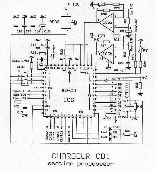
Power section being debunked, it remains to see how it will all come to life. Let us examine Fig. 3. It is the heart of CD1 with a very simple installation. The microcontroller, a 68HC711E9, requires no external components or almost: a crystal for clocking the instructions and some resistance!
Port A controls the display, LED activation IC4. Port B is devoted to the display. Port C is required for the 4-button keypad for control of T1, T2 and blocking IC4. The port D handles signals and IC3 IC4. An extension 232 is considered. Port E is the AD converter. It allows the measurement of - batt, I / load, I / discharge, 12V / E, C. The charge and discharge currents are obtained by the passage of these currents in the resistors R8 and R17 of 0.22 W. Thus a current of 5 A develops a voltage of 5 x 0.22 = 1.10 V. This voltage is too low to cover the dynamic range of AD converter which is 5 V, giving 255 points. Therefore the non-inverting amplifiers IC5 were added. Their gain is about 5 / 1.1, so between 4 and 5. This gain is finalized by the settings P6 and P5 compared with an ammeter outside. IC5 must be said CMOS amplifier "Rail to rail" so as to provide an effective output ranging from 0 to 5V. It is an LMC662. If you want to measure the temperature of the pack, which is not so useful, it will add a little montage similar to amplify the voltages supplied by the sensor LM35. Will be described elsewhere. Of course, the most interesting is not seen! This is the program buried in the ?C. It is an already large with over 1500 lines, of course written in assembler. We understand how frustrating it is for a director to miss that, but we can not do anything. We must simply accept the fact as you agree to use any integrated circuit without really knowing what's going in!
ADDITIONS
* Temperature Probe. The external temperature sensor uses a LM35 associated with an op amp mounted on a printed circuit optional front mounted inside the CD1. This option is described later.
* Charge Schedule. You've probably noticed two banana jack 2mm B1 and B2 on the photo of CD1. These are the outputs of a second assembly load to load optional 4 to 14 elements in a constant current of 120 mA. This output can therefore give a little help from batteries to charge the receiver and / or the transmitter while recharging the battery propulsion. This option is described later. It mounts on the same PCB as the opamp thermal probe.
* RS232. CD1 transmit functions in Charge and discharge all the necessary parameters due to a shipment every minute. A PC can then exploit these results. Software is designed to obtain a curve on the screen charge or discharge. More details later.
* Platinum BUZZER. To activate a buzzer at the end of charge or alarm if the battery charge is connected to upside down or if the battery is disconnected accidentally instantaneous change secure.
* Future extension. CD1 is a medium power charger which is satisfactory for 90% of amateur but we know, some always want more! It will later be possible to move to version CD1 CD2 more muscular. The conversion will be done very easily, keeping the entire base plate except the LT1070. CD1 is in any case a starting safety.
The theoretical study of CD1 is finished, now turn to the realization of the object!
REALIZATION
LIST OF COMPONENTS
MOUNTING
Figure 4 shows the components of the front. If you do not have a circuit with metallized holes, the first job is to make all the passages duplex unrealized by the legs of components. Use wire big enough to power the side passages and the other end. He must think because some are not so obvious. The most difficult lies in the PLCC socket. We must pass the wire end into the holes, fold flat, and weld on the front 2 or 3 mm. Do not weld on the back. When you assemble the PLCC socket, paying careful attention to its direction and move out all the tabs, you solder together with pins and son purposes. Tulip stands for, it's easier because you can easily solder tabs on the front.
Obviously if you have plated through holes is a lot easier! We do not back that soda!
Install all the small parts first, R and C, potentiometers adjustable brackets DILS and PLCC. Solder the connectors HE10: 4 and 5 for females and keyboard leds, 14 male pins for the display. Do not mount IC1 D1, TM1 and TM2. Skip to reverse. Solder the CMS. Install relay, C4, C5, C6, L2. L1 can be mounted, its meaning is irrelevant. Fastons two males for starter and batt + batt.
The connector 5 pin 232 is welded to the back of the circuit board. Note that 3 lines to access the mass, the +5 V and the active output PD1. The socket will receive 3 son and therefore the direction of mating will be indifferent.
At this stage, we must begin commissioning. Do not place any components except the two 78L05.
Check very carefully. Connect the 12V on the input, the son welded on it (-) and below (+). See below Measure the existence of +12 V on 8 of IC2, the relay. Measure the existence of +5 V on pin concerned IC3, IC4, IC5 and IC6. Measure the existence of + 2.5V reference on pin 4 of IC 3. Set P8 to have a voltage of +0.5 V on pin approx 3 of connector display. Crimp the ribbon cable connector 2 x 7 Display. Provide a length of 10 cm. Solder on the display by identifying good wire #.
This picture differs somewhat from the final CD1.
The son will follow in the order. Mount keyboard keys: E (yellow), P (green), + (red) - (blue) on the printed circuit installed sue the front of the housing and held by two bolts 2 mm with 10 mm spacers. Realizing the small flexible cord to 4 son (6 cm), the solder side and a keyboard 5 pin male connector HE10. The LEDs are glued with cyano at the front and fitted with 4 flexible son (10 cm) 4 pin male connector. Make sense marks with dots of paint on these connectors to prevent incorrect connections because they are not undeceived. Final check! 711E9 insert in the right direction. We breathe and .... It connects the 12V in the right direction by observing the display. At the initial moment, the top line is darkened, and the copyright message is written to appear fleetingly on the screen of choice of battery. Retoucher P8 for the best contrast. Press + to move from setting to setting, then - to return. Press P, which makes the cursor disappear, with possible change by + / -. Finish by P to find the blinking cursor. Press E to access the menu.
If all answers correctly, the hardest part: CD1 is alive!
It must complete assembly. Install the elements of the power section. But for this you need the radiator is shown in figure below, to manufacture aluminum 2 mm or more. Note the cons plate which is pierced exactly as the radiator, but with holes large enough to easily pass the bolt heads to be so embedded in its thickness. Fixing the two plates on the caseback is secured by 4 bolts (3 mm holes denoted "f". It will benefit those tapping the radiator forNote first the battery to be treated at the center of the figure. It is connected to contacts of a relay. The diagram shows the relay at rest. Under these conditions the battery is in SHOCK . His pole - is grounded and its positive pole to the circuit of constant current discharge. This circuit consists of N-channel MOSFET controlled by the TM2 IC2B OP amp. The input of this amp + e is at a potential adjustable by the digital potentiometer IC 4. The op amp will therefore act on the conduction of TM2 to pass in R17 to cause sufficient current to equal voltages and e + e-. It is understandable that by adjusting the voltage by e + IC4 is going to vary the intensity of discharge.
The adjustable P4 allows the setting of the value of the intensity at the focus. If it was left to bear the burden of TM2 only the discharge current, it heats up tremendously. In fact, if you release 12 V 2 A 24 W gives it! It would take a huge radiator! We have resolved the issue by inserting the resistors R13 to R15. These resistors are mounted outside the cabinet. These are models with 25 W radiator. The heat does not win inside the CD1. Moreover, it is possible for riders to easily choose 1, 2 or 3 resistors to accommodate the number of items to unload. Fig. 1 Now note the presence of IC3: this is our precision voltmeter! It is 12 bits, thus capable of 4096 points. We calibrate it to measure from 0 to 40.95 V at 1 / 100 of volts. This converter requires an external reference of 2.5 V. Z is the zener (TL431) which provides. The final calibration is done by P1. In discharge mode, the - batt is grounded by the relay, so the voltage measurement is not a problem. Circuits IC4 and IC3 are SERIAL programming. So the ?C which will manage the mission of these two circuits. IC3 is a MAX1241 from MAXIM. IC4 is an AD8402 (10 k W ) ANALOG DEVICES. Readers interested in the functioning of these circuits may, as we did, download the files of these circuits on the Web sites of these manufacturers.
Now to the circuit CHARGE . It is located at the top left of the figure. For charging, the relay switches to work. Consider first the case of charging a battery with small number of elements, such as a 4 elements therefore of 4.8 V. Under these conditions, the input of 12V battery is perfectly sufficient for this load. The circuit IC1 is inactive and the current flows through L1, D1 to return to the ground by the constant current generator built with IC2A and TM1.
This setup is quite similar to that of discharge, with adjustable intensity and IC4 potentiometer 10 k W . Note that the battery will charge to 5.6 V for charge termination. If an estimated loss of 1 V voltage in L1 and D1, it develops a voltage of 12 to 1 - 5.4 = 5.6 V between drain and TM1 mass.
This voltage is fed to the input FB (feedback) of IC1 and as this voltage exceeds 1.25 V, this circuit is blocked Now imagine a battery of 12 elements is about 18 V charge termination. This time, the 12 V input are unable to impose their law! The charge current is zero at the initial moment. This FB is at 0 V. So IC1 wakes and begins his work! The circuit IC1, a LT1070C of LINEAR TECHNOLOGIES DC-DC converter: it converts a DC voltage (DC) to another (DC).
Here he works in "boost", which means that the outgoing voltage is higher than the incoming. Why is this small miracle? If we look at the internal structure of IC1, see Fig. 2, we find that the output Vsw can be connected to ground through internal transistor. Conduction of this transistor is obtained using an internal oscillator 40 kHz variable duty cycle and function of the voltage on the FB pin. When the transistor conducts, the 12V back to the ground through L1. The coil, said storage stores energy in magnetic form. When the transistor is blocked, said energy is converted back into voltage (the famous power failure giving sparks!) Direction as it goes into the series with 12 V input voltage onto C4 than 12 V.
To increase the tension, increase the time of the grounding of L1 and vice versa. The double diode D1 prohibits the discharge of C4 to L1 and IC1. Fig. 2 In our experiments, the LT1070 is controlled by the charging current . The LT1070 raises the output voltage until the battery to be charged, sufficient current for 1.25 V across the constant current generator, or TM1 + R8. This system is particularly attractive because the voltage coming out of the boost converter is always just enough to have the intensity set, through IC4.
Finally, the potential difference between input and 12V + batt is minimal, which allows a moderate heat dissipation and therefore requires no bulky radiators. The temperature rise is minimal when the battery charge has a voltage of about 12V, which is the case pack of 7 to 10 cells: Little work for IC1 and low voltage drop in TM1 and R8.
When the number of elements is small, no heating of IC1 but cons TM1 cash voltage difference and heaters more. When the number of elements is greater than 10, the LT1070 is utilized and tends to heat, but low dissipation TM2.
At rest the relay, the LT1070 is powered but the output circuit is opened and the FB voltage to zero. Under these conditions, IC1 will tend to get carried away, trying to mount FB, unsuccessfully of course.
Carelessly it goes very fast and IC1 passes away with a significant release of noxious smoke. It was then that we understand the role of T1: By making the LT1070 driver is blocked and it saves him from disaster! The presence of the relay can worry. Risk of sparks? No, for this relay is always zero switching, both support that defense. A delay of 1 s is allowed before and after each passage or failure of the currents. Note the presence of D2, which prohibits the relay coil to create dangerous overvoltages cuts for T2.
Here we wish to avoid precisely what we sought with L1! IC3 IC4 and are supplied by 5 V REG1, a 78L05. L2 C6 and perform filtering of 12V which is quite disturbed by the fact that cutting IC1. The voltage of the battery charge is monitored very carefully by our voltmeter IC3. However, the beats-not to ground but often close to a voltage of 1.25 V, but can climb higher with little evidence to charge (see above). So we need to measure the voltage-batt and deduct from that of + batt for the battery voltage accurately.
A second voltmeter is required. This is one of the inputs of the converter's internal 711E9 has this mission: PE0. It actually measures low voltages into 8 bits, which is sufficient. To be assured of complete accuracy with the necessary technical DELTA-PEAK actually performs the ?C 16 consecutive measurements of + batt-batt and 16. Are tabulated and divided by 16! The most formidable of this is that the measures require 16 + 16 ms ... 4! Another important point: The voltage measurements are charging current cut . The length of the son from the battery to charge to CD1 is not very critical, which is not the case with some commercial shippers!
Finally all these precautions are the measures undertaken by CD1 have excellent accuracy, with displays very stable! A real treat! Power section being debunked, it remains to see how it will all come to life. Let us examine Fig. 3. It is the heart of CD1 with a very simple installation. The microcontroller, a 68HC711E9, requires no external components or almost: a crystal for clocking the instructions and some resistance!
Port A controls the display, LED activation IC4 Port B is devoted to the display Port C is required for the 4-button keypad for control of T1, T2 and blocking IC4 The port D handles signals and IC3 IC4. An extension 232 is considered. Port E is the AD converter. It allows the measurement of-batt, I / load, I / discharge, 12V / E, C The charge and discharge currents are obtained by the passage of these currents in the resistors R8 and R17 of 0.22 W .
Thus a current of 5 A develops a voltage of 5 x 0.22 = 1.10 V. This voltage is too low to cover the dynamic range of AD converter which is 5 V, giving 255 points. Therefore the non-inverting amplifiers IC5 were added. Their gain is about 5 / 1.1, so between 4 and 5. This gain is finalized by the settings P6 and P5 compared with an ammeter outside. IC5 must be said CMOS amplifier Fig 3 "Rail to rail" so as to provide an effective output ranging from 0 to 5V. It is an LMC662. If you want to measure the temperature of the pack, which is not so useful, it will add a little montage similar to amplify the voltages supplied by the sensor LM35.
Will be described elsewhere. Of course, the most interesting is not seen! This is the program buried in the ?C. It is an already large with over 1500 lines, of course written in assembler. We understand how frustrating it is for a director to miss that, but we can not do anything. We must simply accept the fact as you agree to use any integrated circuit without really knowing what's going in! ADDITIONS <<<
This option is described later. * Charge Schedule. You've probably noticed two banana jack 2mm B1 and B2 on the photo of CD1 These are the outputs of a second assembly load to load optional 4 to 14 elements in a constant current of 120 mA. This output can therefore give a little help from batteries to charge the receiver and / or the transmitter while recharging the battery propulsion.
This option is described later. It mounts on the same PCB as the opamp thermal probe * RS232 . CD1 transmit functions in Charge and discharge all the necessary parameters due to a shipment every minute. A PC can then exploit these results. Software is designed to obtain a curve on the screen charge or discharge. More details later. * Platinum BUZZER . To activate a buzzer at the end of charge or alarm if the battery charge is connected to upside down or if the battery is disconnected accidentally instantaneous change secure.
* Future extension. CD1 is a medium power charger which is satisfactory for 90% of amateur but we know, some always want more! It will later be possible to move to version CD1 CD2 more muscular. The conversion will be done very easily, keeping the entire base plate except the LT1070. CD1 is in any case a starting safety. The theoretical study of CD1 is finished, now turn to the realization of the object! REALIZATION LIST OF COMPONENTS <<<
Tulip stands for, it's easier because you can easily solder tabs on the front. Obviously if you have plated through holes is a lot easier! We do not back that soda! Install all the small parts first, R and C, potentiometers adjustable brackets DILS and PLCC Solder the connectors HE10: 4 and 5 for females and keyboard leds, 14 male pins for the display. Do not mount IC1 D1, TM1 and TM2. Skip to reverse. Solder the CMS. Install relay, C4, C5, C6, L2. L1 can be mounted, its meaning is irrelevant. Fastons two males for starter and batt + batt. Fig. 4 ( click to view Verso ) The connector 5 pin 232 is welded to the back of the circuit board.
Note that 3 lines to access the mass, the +5 V and the active output PD1. The socket will receive 3 son and therefore the direction of mating will be indifferent. At this stage, we must begin commissioning. Do not place any components except the two 78L05. Check very carefully. Connect the 12V on the input, the son welded on it (-) and below (+). See below Measure the existence of +12 V on 8 of IC2, the relay. Measure the existence of +5 V on pin concerned IC3, IC4, IC5 and IC6. Measure the existence of + 2.5V reference on pin 4 of IC 3. Set P8 to have a voltage of +0.5 V on pin approx 3 of connector display Crimp the ribbon cable connector 2 x 7 Display. Provide a length of 10 cm. Solder on the display by identifying good wire # This picture differs somewhat from the final CD1 .
The son will follow in the order. Mount keyboard keys: E (yellow), P (green), + (red) - (blue) on the printed circuit installed sue the front of the housing and held by two bolts 2 mm with 10 mm spacers. Realizing the small flexible cord to 4 son (6 cm), the solder side and a keyboard 5 pin male connector HE10.
The LEDs are glued with cyano at the front and fitted with 4 flexible son (10 cm) 4 pin male connector. Make sense marks with dots of paint on these connectors to prevent incorrect connections because they are not undeceived.
Final check! 711E9 insert in the right direction. We breathe and .... It connects the 12V in the right direction by observing the display. At the initial moment, the top line is darkened, and the copyright message is written to appear fleetingly on the screen of choice of battery. Retoucher P8 for the best contrast. Press + to move from setting to setting, then - to return. Press P, which makes the cursor disappear, with possible change by + / -. Finish by P to find the blinking cursor. Press E to access the menu. If all answers correctly, the hardest part: CD1 is alive! It must complete assembly. Install the elements of the power section. But for this you need the radiator is shown in figure below, to manufacture aluminum 2 mm or more. Note the cons plate which is pierced exactly as the radiator, but with holes large enough to easily pass the bolt heads to be so embedded in its thickness.
Fixing the two plates on the caseback is secured by 4 bolts (3 mm holes denoted "f". It will benefit those tapping the radiator for easy installation. The LT1070 is mounted directly, but D1, TM1 and TM2 should be isolated in the rules. A little paste special radiator is welcome to promote heat exchange. The radiator plate and cons must be mounted so that they come back exactly at the long edge of the PCB. Mount the assembly on the plate, screws loosely, thereby facilitating the threading of all the legs. Check position and welded. Tighten the screws. Connect the two resistors. The rear of the radiator must be applied to the back of the unit prepared and on which it is bolted (See the four holes "f" Radiator).
Predict thermal grease. The case contributes to the effect radiator. Install discharge resistors, R13 to R14 on an aluminum plate of 2 mm. The junctions between resistors are made with added sockets miniature 1 mm. The plate is mounted on the case back on spacers of 5 mm and 2.5 mm bolts. 🔗 External reference
Related Circuits
This is a relay circuit that detects the presence of sound to activate the relay. This sound-controlled relay can be utilized as a voice-operated switch or for controlling lights. The sound-activated relay circuit typically employs a microphone or a sound...
The schematic diagram originates from a circuit designed for a Car Lamp Charger power supply. The diagram illustrates a Car Lamp Charger circuit, which features a unique characteristic: the battery will not recharge. This circuit is integrated into a...
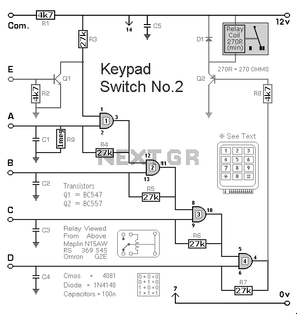
The Keypad Controlled Switch No2 Circuit operates with a 12-volt supply but is compatible with voltages ranging from 5 to 15 volts. The only requirement is to select a relay that matches the desired supply voltage. The Keypad Controlled Switch...
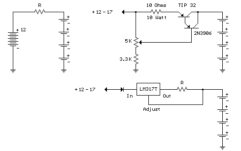
A simple method for charging a battery from a higher voltage battery is illustrated in the circuit below on the left. Only one resistor is required to establish the desired charging current, which is determined by dividing the difference...
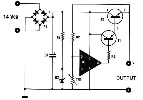
This automatic battery charger circuit is ideal for charging batteries used in alarm systems that require battery buffering. Caution must be exercised when connecting the battery to ensure correct AC polarity. It is essential to meticulously follow the schematic...
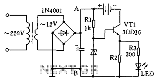
A practical single-tube constant current charger is illustrated, utilizing a transistor (VT1) that plays a crucial role in maintaining a constant current. The current value is determined by the voltage regulator and resistor R2. The general output voltage is...