
fast voltage driven current source
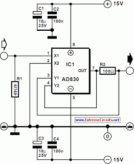
The circuit described encompasses a high-speed current source designed to respond rapidly to variations in the input signal, making it suitable for precise measurement applications. The differential amplifier IC1 plays a critical role in maintaining the voltage across resistor R2 equivalent to the input voltage, facilitating accurate current output calculations. The relationship Iout = Uin/R2 indicates that the output current is directly proportional to the input voltage and inversely proportional to the resistance of R2.
The bandwidth of the system, determined by the formula B = R2 f / RL, highlights the importance of both the resistance R2 and the load impedance RL in defining the frequency response of the circuit. With a specified frequency of 80 MHz, it is essential that the load impedance RL meets or exceeds the value of R2 to ensure optimal performance.
Resistor R1 serves a dual purpose in the circuit. It not only provides the necessary termination for the input signal, ensuring a standard 50-ohm impedance for compatibility with measuring instruments, but it also establishes the DC operating point of the circuit. In scenarios where the connection to the driving signal source is short and DC coupled, R1 can be omitted, simplifying the circuit design without compromising performance.
To safeguard the circuit from excessive output current, the peak voltage between the pins of the differential amplifier is limited to 2.1 V. This design consideration is crucial, as it prevents potential damage to the output stage of the amplifier. Consequently, the peak output current is calculated to be 21 mA, derived from the voltage limitation divided by the resistance of 100 ohms, ensuring that the current remains within safe operational limits. Overall, this circuit configuration is engineered for high-speed applications while maintaining stability and protection against overcurrent conditions.The current source in the diagram, which react very fast to changes in the input signal, may be used, for instance, in certain measurements. Differential amplifier IC1 ensures that the potential across R2 is equal to the input voltage: Iout =Uin/R2.
The bandwidth, B, is given by B=R2 f /RL, where f=80 MHz, and the load impedance RL‰¥ R2 (both in ohms). The input is terminated into R1 to give the usual 50 impedance required by measuring instruments. At the same time, this resistor sets the d. c. operating point. If the link to the driving signal source is short and d. c. coupled, R1 may be omitted. The peak voltage between pins 1 and 2 of the IC is limited to 2. 1 V to prevent too large a current at the output. Therefore, the peak output current is 2. 1/100=21 mA. 🔗 External reference
Related Circuits
The schematic shows R4 at the emitter of the transistor, as suggested by Amb and Majkel. It should be positioned between the operational amplifier and the transistor, which is also the correct configuration in the CanAmp. The amplifier observed...
The input terminal VIN is connected to the +V line of the circuit that the indicator is meant to monitor, and the grounds of both circuits are interconnected. The position of the potentiometer R1's wiper determines the base voltage...

This circuit requires a control current that is 100 times smaller than that required by standard optically isolated solid-state relays. It is particularly suitable for battery-powered systems. By utilizing a combination of a high-current TRIAC and a very sensitive...

The circuit possesses significant educational value. It has not been tested. Users can simulate and test it or construct it to evaluate its performance. The circuit functions as a simple analog-to-digital converter. Optocouplers can be used in place of...
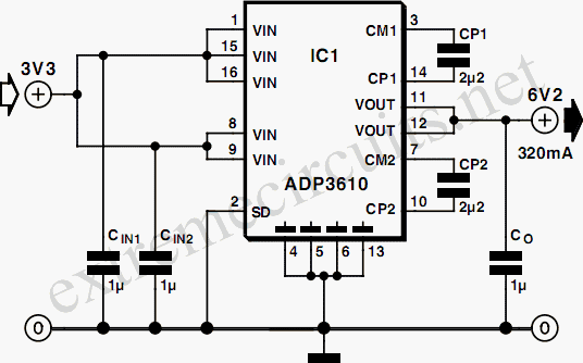
The Analog Devices ACP3610 is a voltage doubler that operates using a switched-capacitor converter based on the push-pull principle. The output switching frequency is approximately 550 kHz. The push-pull configuration involves two charge pumps that function in parallel but...
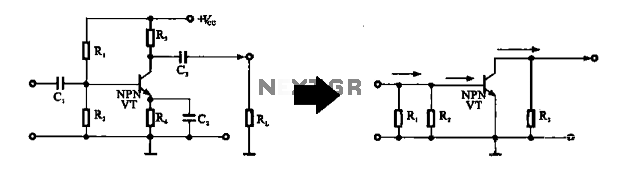
An alternating current voltage amplifier transistor AC path is described. In AC analysis, the internal resistance of the AC supply voltage source is low, which corresponds to a short circuit signal. Consequently, the alternating voltage terminal Vcc is considered...
Warning: include(partials/cookie-banner.php): Failed to open stream: Permission denied in /var/www/html/nextgr/view-circuit.php on line 713
Warning: include(): Failed opening 'partials/cookie-banner.php' for inclusion (include_path='.:/usr/share/php') in /var/www/html/nextgr/view-circuit.php on line 713