
Switching Voltage Regulator
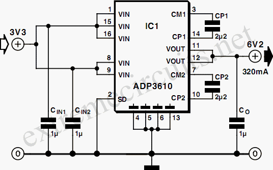
The ACP3610 voltage doubler is designed for applications requiring efficient voltage conversion with minimal ripple and loss. Its architecture utilizes a dual charge pump system that alternates between charging and discharging, allowing for continuous power delivery. The design emphasizes the importance of selecting capacitors with low ESR to ensure that the voltage doubler operates within its optimal parameters. The low ESR capacitors not only enhance the efficiency of the charge pumps but also stabilize the output voltage against fluctuations caused by load changes.
The shutdown feature is particularly useful in battery-operated devices, where power conservation is critical. By controlling the enable pin, the device can be turned off when not in use, significantly reducing power consumption.
In terms of layout considerations, the placement of the input and output capacitors should be as close as possible to the IC pins to minimize inductance and resistance in the circuit. This practice will further enhance the performance of the voltage doubler by reducing voltage spikes and ensuring stable operation under varying load conditions.
For applications where higher output currents are required, multiple ACP3610 devices can be paralleled, provided that appropriate load-sharing techniques are implemented to ensure balanced current distribution among the devices. This scalability allows for flexibility in design, accommodating a wide range of output power requirements.
Overall, the ACP3610 represents a robust solution for voltage doubling applications, combining high efficiency, compact size, and ease of integration into various electronic systems.The Analog Devices ACP3610 is a voltage doubler that works with a switched-capacitor converter, using the push-pull principle. The switching frequency at the output is approximately 550 kHz. The term push-pull` refers to the two charge pumps, which work in parallel but in opposite directions in order to deliver the output voltage and current.
When ever one capacitor is supplying current to the output, the other one is being charged. This technique minimizes voltages losses and output ripple. The converter works with input voltages between 3 and 3. 6 V. It provides an output voltage of around 6V at a maximum current of 320mA, if 2. 2 µF switched capacitors with low ESR (equivalent series resistance) are used. A shut-down input is provided to allow the voltage doubler to be enabled or disabled by a logic-level signal. The IC is enclosed in a special package, which can dissipate up to 980mW at room temperature. The schematic diagram shows a typical application for the ADP3610. Here it works as a non-regulated voltage doubler. In theory, a voltage doubler can provide exactly twice the input voltage at its output, but in practice the combination of internal losses in the electronic switches and the internal resistances of the capacitors always causes the output voltage to be somewhat lower.
The output voltage drops from a no-load value of 6 V to 5. 4 V with a 320mA load, with a nearly linear characteristic. A small capacitor is connected across the two supply pins at the input of the IC. It suppresses noise, brief voltage‚uctuations, and current peaks when the ADP3610 switches. This capacitor (CIN) must have a low internal resistance (ESR). A larger capacitance value is necessary if long supply leads to the ADP3610 are present. The 1 µF output capacitor (CO) is alternately charged by the two capacitors of the charge pump, CP1 and CP2. The internal resistance is an important factor here as well. It largely determines the amount that the voltage drops under load, and the amount of ripple in the output voltage.
Ceramic or tantalum capacitors are recommended. The ESR can also be reduced by connecting several smaller-value capacitors in parallel. With small loads, the value of CO may be reduced. 🔗 External reference
Related Circuits
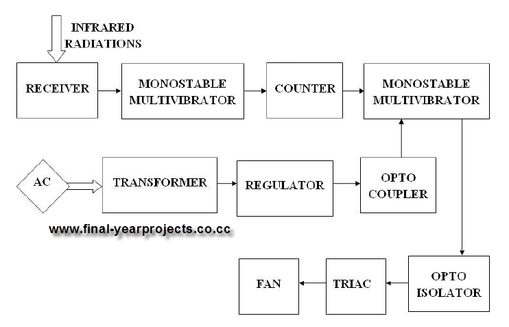
This report presents a comprehensive overview of a mini project titled "Remote Controlled Fan Regulator," developed in accordance with the curriculum requirements for the sixth semester of the Bachelor of Technology degree in Electrical and Electronics Engineering. The report...
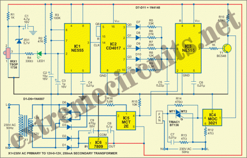
This circuit allows for the adjustment of fan speed from a distance, such as from a couch or bed. It utilizes the TSOP1738 infrared receiver module to capture the infrared signals. The circuit operates by employing an infrared remote control,...
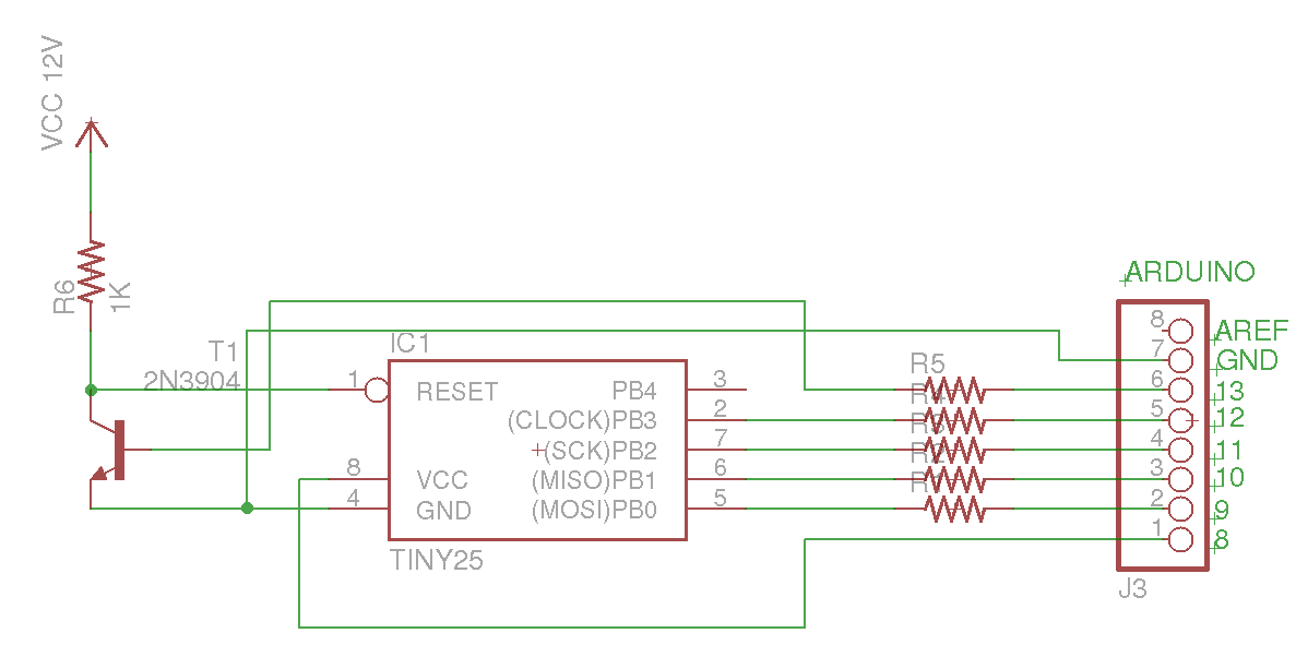
This Arduino sketch is designed to recover ATtiny microcontrollers that have become non-functional due to incorrect fuse settings. It achieves this by placing the affected ATtiny into high-voltage serial programming mode and rewriting the fuses to safe values. The...
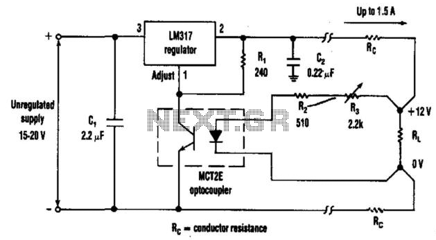
The optocoupler provides load sensing for a 3-terminal regulator, such as the LM317 series. Rl sets a current of 5 mA through the optocoupler transistor, and R3 is adjusted for 12 V across the load. The circuit utilizes an optocoupler...
This project is designed to prevent unauthorized access to personal belongings left on a beach towel while swimming, and it can also be utilized in office or workshop settings. The circuit is compact and can be powered by simple...
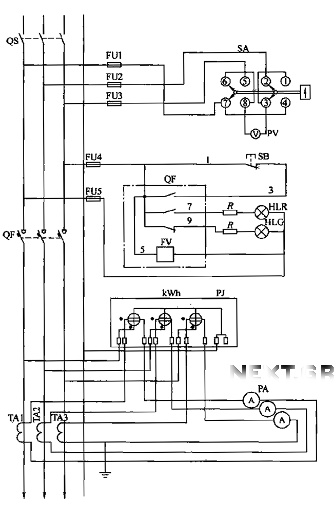
The BSL is illustrated in a low-voltage distribution panel wiring diagram. It consists of three main components: the voltage measuring circuit, secondary circuit protection, and the energy metering circuit. (1) The voltage measuring circuit includes a voltage switch (SA)...