
FET applications

1. Low Noise Amplifier: Noise is an unwanted disturbance superimposed on a useful signal, which can obscure the information contained within that signal. For example, noise in radio receivers can create crackling and hissing sounds that mask audio content, while noise in television receivers may result in small white or black spots on the display. All electronic devices generate some level of noise; however, FETs produce minimal noise, making them particularly valuable at the front end of receivers and other electronic systems. This is crucial because subsequent stages amplify both the signal and any front-end noise. Utilizing FETs at the front end results in reduced amplified noise in the final output. A buffer amplifier serves to isolate one stage of amplification from another. The source follower configuration (common drain) acts as an effective buffer amplifier due to its high input impedance and low output impedance. Consequently, nearly all output voltage from the preceding stage is present at the buffer amplifier's input, and the low output impedance ensures that the output voltage from the buffer reaches the next stage, even with a small load resistance.
2. Cascode Amplifier: The cascode amplifier configuration offers the same voltage gain as a common source (CS) amplifier. The primary advantage of the cascode arrangement lies in its low input capacitance, which is significantly less than that of a CS amplifier. Additionally, it boasts high input resistance, which is a beneficial characteristic.
3. Analog Switch: The FET can also function as an analog switch. When no gate voltage is applied (VGS = 0), the FET enters saturation and behaves like a small resistance, typically less than 100 ohms, causing the output voltage to equal the input voltage. Conversely, when a negative voltage equal to VGS (OFF) is applied to the gate, the FET operates in the cutoff region and behaves like a very high resistance, often in the megaohm range, resulting in the output voltage being nearly equal to the input voltage.
4. Chopper: A direct-coupled amplifier can be constructed by omitting coupling and bypass capacitors, thereby directly connecting the output of one stage to the input of the next. This configuration allows for the coupling of both direct current (DC) and alternating current (AC). However, a significant drawback of this method is the occurrence of drift, which is a gradual shift in the final output voltage caused by supply transistors and temperature variations. In this setup, an input DC voltage is chopped by a switching circuit, producing an output that is a square wave AC signal with a peak value equal to the input DC voltage (VDC). This AC signal can be amplified by a conventional AC amplifier without the issues associated with drift. The amplified output can then be peak detected to recover the amplified DC signal. A square wave applied to the gate of a FET analog switch allows it to operate as a chopper. The gate square wave swings negatively from 0 V to at least VGS (off), alternately saturating and cutting off the JFET. Consequently, the output voltage becomes a square wave that varies from +VDC to zero volts.FET has a very high input impedance (100 Mega ohm in case of JFETs and 104 to 109 Mega Ohm in case of MOSFETs), the major shortcomings of an ordinary transistor i. e. low input impedance with consequent of loading of signal source is eliminated in FET. Hence FET is an ideal device for use in almost every application in which transistors can be used . FETs are widely used as input amplifiers in oscilloscopes, electronic voltmeters and other measuring and testing equipment because of their high input impedance. FETs are used as voltage-variable resistors (WRs) in operational amplifiers (op-amps) and tone controls etc, for mixer operation on FM and TV receivers and in logic circuits.
1. Low Noise Amplifier. Noise is an undesirable disturbance super-imposed on auseful signal. Noise interferes with the information contained in the signal; the greaterthe noise, the less the information. For instance, the noise in radio-receivers developscrackling and hissing which sometimes completely masks the voice or music.
Similarly, the noise in TV receivers produces small white or black spots on the picture; a severe Every electronic device produces certain amount of noise but FET is a device which causes very little noise. This is especially important near the front-end of the receivers and other electronic equipment because the subsequent stages amplify front-end noise along with the signal.
If FET is used at the front-end, we get less amplified noise (disturbance) at the final output. A buffer amplifier is a stage of amplification that isolates thepreceding stage from the following stage. Source follower (common drain) is. used as abuffer amplifier. Because of the high input impedance and low output impedance a FETacts an excellent buffer amplifier, as shown in figure.
Owing to high input impedance almost all the output voltage of the preceding stage appears at the input of the buffer amplifier and owing to low output impedance all the output voltage from the buffer amplifier reaches the input of the following stage, even there may be a small load resistance. The cascode amplifier has the same voltage gain as a common source (CS) amplifier. The main advantage of cascode connection is its low input capacitance which is considerably less than the input capacitance of a CS amplifier.
It has high input resistance which is also a desirable feature. 4. Analog Switch. FET as an analog switch is shown in figure. When no gate voltage is applied to the FET i. e. VGS = 0, FET becomes saturated and it behaves like a small resistance usually of the value of less than 100 ohm and, therefore, output voltage becomes equal to When a negative voltage equal to VGS (OFF) is applied to the gate, the FET operates in the cut-off region and it acts like a very high resistance usually of some mega ohms. Hence output voltage becomes nearly equal to input voltage. 5. Chopper. A direct-coupled amplifier can be built by leaving out the coupling and bypass capacitors and connecting the output of each stage directly to the input of next stage.
Thus direct current is coupled, as well as alternating current. The major drawback of this method is occurrence of drift, a slow shift in the final output voltage produced by supply transistor, and temperature variations. (a). Here input dc voltage is chopped by a switching circuit. The output of chopper is a square wave ac signal having peak value equal to that of input dc voltage, VDC.
This ac signal can be amplified by a conventional ac amplifier without any problem of drift. Amplified output can then be peak detected` to recover the amplified dc signal. Square wave is applied to the gate of a FET analog switch to make it operate like a chopper, as illustrated in other figure. The gate square wave is negative-going swing from 0 V to at least VGS (off)- This alternately saturates and cuts-off the JFET.
Thus output voltage is a square wave varying from +VDC to zero vol 🔗 External reference
Related Circuits
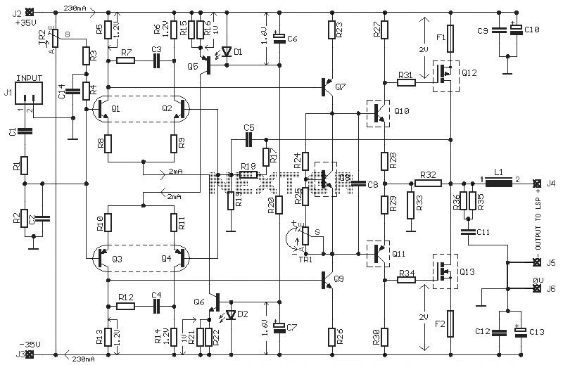
This HEXFET Audio Amplifier 65 Watts circuit diagram includes three circuit images. For a more comprehensive understanding, refer to the original post titled "HEXFET Audio Amp 65 Watts." The post not only provides circuit information but also includes a...
A Darlington transistor can enhance circuit performance, although it introduces slight complexity. The advantage of using a Darlington configuration lies in its capability to achieve low output impedance. The recommended component is the 2N6426 from Mouser, with alternatives such...
This is an On After Delay Circuit. It utilizes a MOSFET in the circuit for easier delay implementation compared to using a transistor. The operation of the circuit begins when switch S1 is pressed. The On After Delay Circuit is...
Can be directly connected to CD players, tuners and tape recorders. Simply add a 10K Log potentiometer (dual gang for stereo) and a switch to cope with the various sources you need. A correct grounding is very important to...
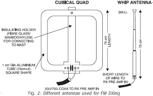
FM transmissions can be received within a range of 40 km. In fringe areas, the signal may be very weak. FM DXing refers to the practice of receiving distant stations (1500 km or more) on the FM band (88-108...
Capacitors C1 and C2, in conjunction with a speed controller, function by receiving voltage at the gate of the MOSFET. When the voltage on C is applied, it activates the operation of the MOSFET. In this circuit configuration, capacitors C1...