
Few words about CPLD
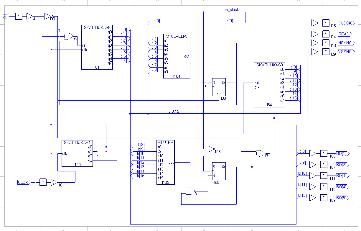
The project centers around the implementation of a programmable logic device, specifically the Lattice isp2032VE110LT144 chip, to control an LCD screen module without a microcontroller. The integration process began with the soldering of the chip onto a custom-designed printed circuit board (PCB). The programming environment utilized was ispLever Navigator, which facilitates the development of complex digital systems.
To initiate the project, a mixed design approach was adopted, utilizing both ABEL and schematic representations. This choice allowed for the flexibility of defining certain modules in ABEL, which is a high-level hardware description language, while also leveraging the graphical capabilities of the schematic editor to interconnect the various components. The primary challenge addressed was generating the necessary timing signals for the LCD operation, specifically the clock, vertical sync (vsync), and horizontal sync (hsync) signals.
Row and column detection modules were crafted to manage the addressing of the LCD. In the ABEL language, modules are defined with mandatory fields, including the module name, variable declarations, and the logic equations that govern their functionality. The row detection logic was implemented through a specific ABEL file, while the column detection logic mirrored this structure.
A significant aspect of the design involved the use of binary counters. A 4-bit counter was employed to divide the master clock frequency, simplifying the logic from existing examples. In contrast, an 8-bit counter was designed with a reset functionality, adding complexity to the timing control. The ispLever software was instrumental in generating schematic symbols from the ABEL scripts, which could then be integrated into the overall circuit design.
Simulation capabilities provided by the software allowed for extensive testing of the circuit. However, the simulation of the LCD logic required substantial computational power due to the high volume of clock cycles needed to replicate full-screen timings. This necessitated a robust computer system to manage the simulation effectively.
Once the logical design was validated through simulation, the Constraint Editor was utilized to assign the necessary signals to the physical pins of the Lattice chip. Although pin assignments could be described in ABEL, the graphical interface offered a more intuitive method for making adjustments. The final programming of the chip was executed using the LSC ispVM System software via a JTAG interface, enabling real-time testing and modifications.
Despite the progress made, the limitations of the isp2032VE110LT144 chip's memory capacity hindered the project's completion. The potential for future development exists with the transition to a field-programmable gate array (FPGA), which would provide greater resources and flexibility for the project. The current state of the project includes a visual display from the LCD screen, albeit with limitations, indicating the need for further enhancements and optimizations.I forced myself to use and learn about programmable logic chips. As I wrote in my older post, I have very small inventory of the chips and was forced to use Lattice isp2032VE110LT144 chip. I received great help reading article from Seattle Robotics Society web page. Also, at same time I was experimenting with controller-less LCD screen module. So I joined both ideas to one project and here is the result. The theory about LCD control was tested using big computer and MS Visual Basic software. CPLD programing software I downloaded from Lattice Semiconductors site. The chip was soldered to self-made testing PCB. I started ispLever Navigator and started my project from nill. I not too smart to wrote all signals is HDL (hardware description language) so I selected mixed type of the project: ABEL + Schematics. So I can describe some modules in ABEL language and connect all modules using graphics editor in schematics editor.
I selected ABEL as I had some examples already written in it. In theory I need to feed LCD with clock, vsync and hsync pulses. It is very easy to describe column and row detection logic modules. Here is row detector (eiles. abv) In ABLEL language there are few mandatory fields: MODULE name of the module; declarations- declaration of the variables and wires; equations- the logic formulas itself. In this example we use whole bunch of wires or bus called a[] a8, a9, a10 and etc. up to a15. I collected wires to bus for easy description. In equations section we just test the bus for some value. The column detect is identical (stulpai. abv): The binary counter is a bit more complicated. I use two types of counters in this project- one is 4 bit counter for dividing frequency of master clock (count4.
abl): This counter is created using example. I only simplified it. It just divides the master clock. Other counter is more complicated- it has reset pin (count8. abl): IspLever software generate schematic symbols from these scripts and they can be placed into circuit diagram as components. So I added some standard logic and here is the result: It is possible to simulate and test the circuit just using software in your computer.
There is special software for this and you can watch all oscillograms on the screen. The problem is, that to test all LCD logic the computer must simulated whole screen timings- tens of thousands of clock tics. It took lots of memory and time in computer. You must have quick one. Now we can star Constraint Editor and connect all signals to real pins of the chip. It is possible to describe pins in ABEL language, but is much easier to do it in graphic interface. And it much more easier to change the pins in visual way. Now start LSC ispVM System program and program real chip using JTAG cable. And now time for experiments and fine tuning of the project- just change, recompile and reprogram the chip.
The chip can be reprogrammed tens of thousands times, so don`t worry. In the image you can see part of the LCD screen with chaotic image. This image is generated from ROM chip- it is used as video RAM . But the project is closed as the chip is too small for this project. Maybe I`ll finish this project using FPGA chip. 🔗 External reference
Related Circuits
Complex programmable logic devices (CPLDs) contain the building blocks for hundreds of 7400-series logic ICs. Complete circuits can be designed on a PC and then uploaded to a CPLD for instant implementation. CPLDs are integrated circuits that provide a versatile...
The resonator appears to be highly susceptible to harmonics. For instance, if the resonator frequency is set at 455 kHz, it also permits frequencies at 910 Hz, 1820 kHz, and 3.640 MHz, which seems to be dominant. Frequencies around...
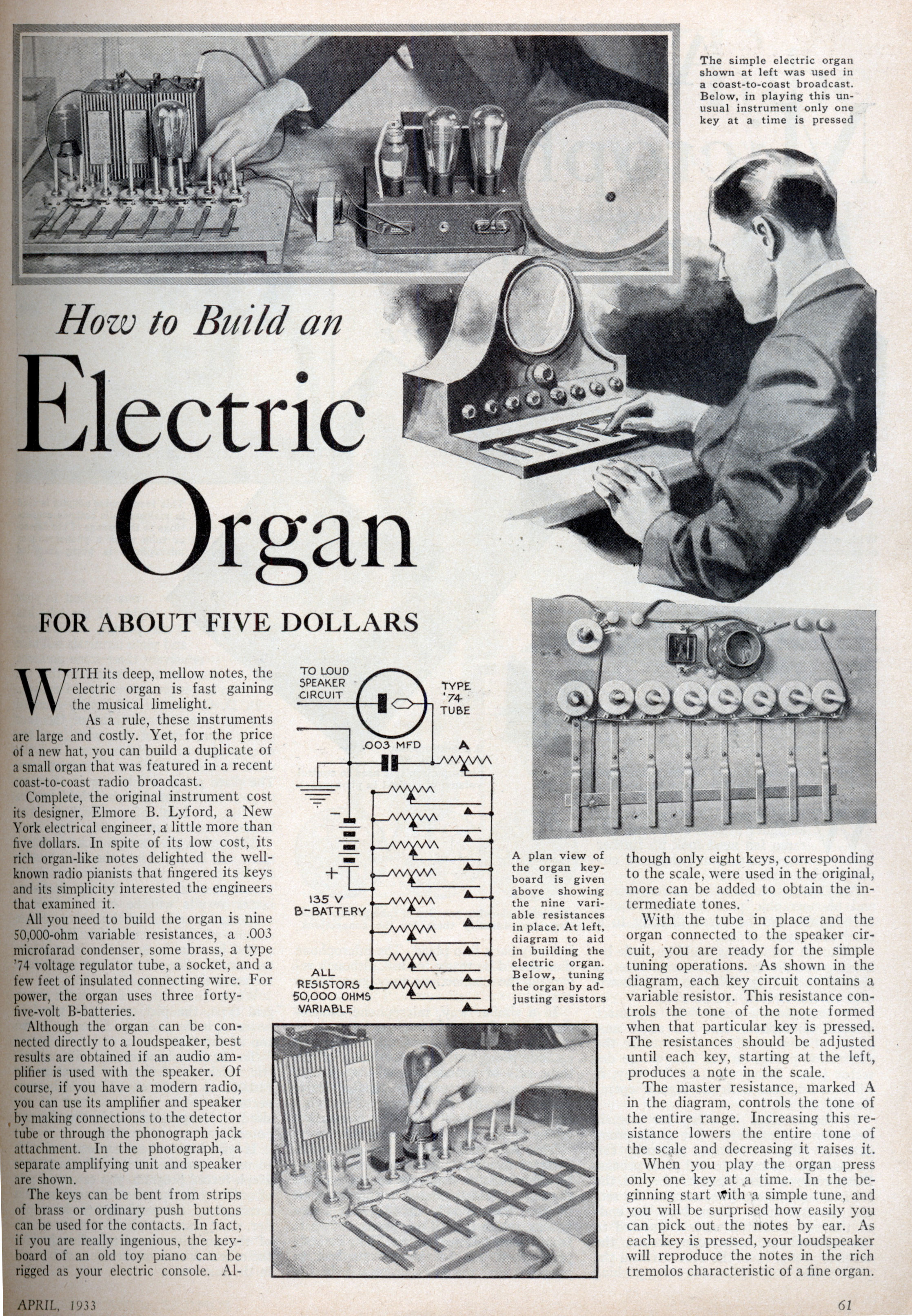
With its deep, mellow tones, the electric organ is rapidly gaining popularity in the music scene. Typically, these instruments are large and expensive. However, for the price of a new hat, one can construct a miniature version of an...
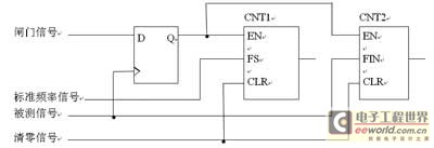
This digital frequency meter circuit is concise, with its software capabilities fully utilized. It achieves high survey accuracy in the low-frequency band while effectively preventing interference. The unique quality is demonstrated by replacing hardware components with software solutions. VHDL...
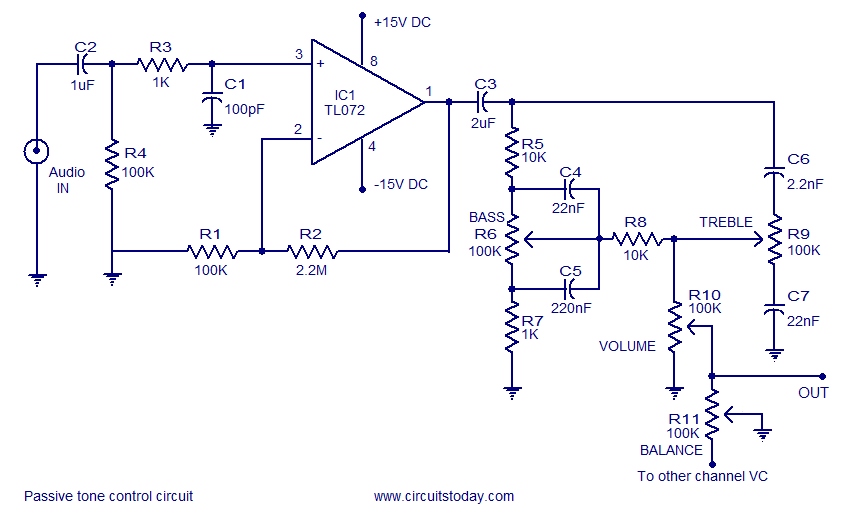
Tone control circuit utilizing an operational amplifier and a Baxandall passive tone control configuration. The overall gain is 25 dB, with a boost and cut capability of 20 dB. The circuit is powered by a dual 15V supply. The tone...
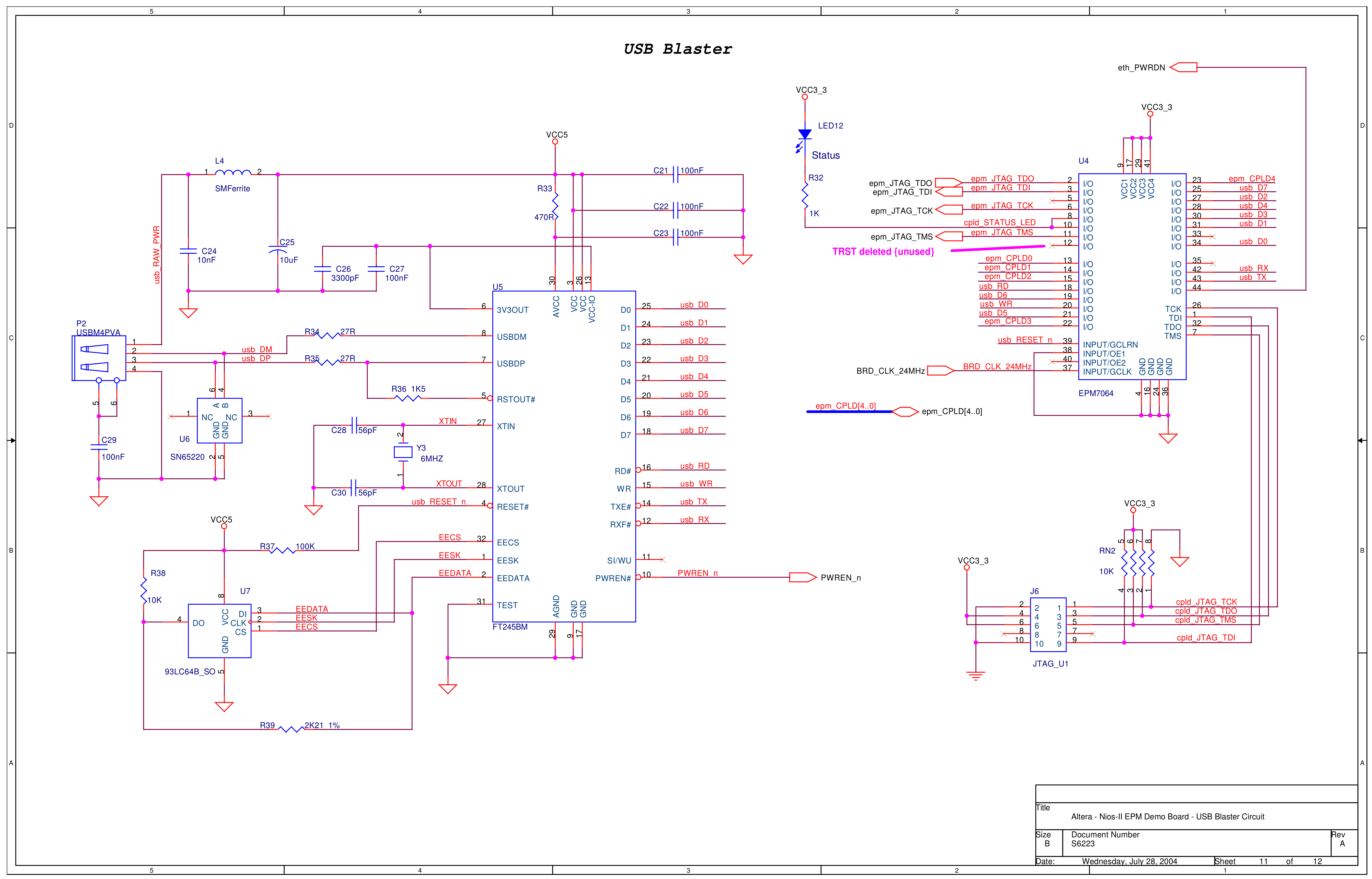
This programming interface circuit transmits programming signals from a USB cable directly to an FPGA chip via a standardized 10-pin interface. Typically, only 4 or 5 signal pins are utilized, excluding GND and any unused pins from the 10-pin...