
Flip-Flop Using CMOS NAND Gates
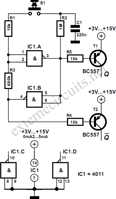
The described circuit utilizes two NAND gates or inverters to create a toggle flip-flop configuration, effectively allowing for a simple and efficient method of storing a binary state. The operation begins with the initial state of gate N2 being high (logic 1) at power-up, which keeps transistor T2 in an off state. This configuration ensures that no current flows through T2 until the push-button is activated.
Upon pressing the push-button, the output of N2 transitions to a low state (logic 0), which activates T2 and allows current to flow. The feedback mechanism established between N1 and N2 guarantees that the output of N1 is always the opposite of N2. This complementary behavior causes the flip-flop to toggle its state with each button press, effectively changing the state of T1 and T2 alternately.
While it is feasible to connect external circuits directly to the outputs of N1 and N2, this is only advisable when the load is minimal, as the 4000 series CMOS gates can handle a maximum of 0.5 mA. To ensure reliability and prevent potential damage, it is recommended to use open-collector transistor buffers for higher loads.
Furthermore, when integrating this circuit into a larger design, it is essential to connect any unused CMOS gates to either the positive supply or ground. This practice prevents floating inputs that could lead to unpredictable behavior. The operational voltage for this circuit can range from 3 V to 15 V, making it versatile for various applications, while the current consumption remains low, typically between 0.2 mA and 5 mA under no-load conditions. This circuit design is especially advantageous for applications where space is limited, and existing components can be repurposed, thus eliminating the need for additional flip-flop integrated circuits.Using just two NAND or inverter gates its possible to build a D type (or toggle`)‚ip-‚op with a push-button input. At power-up the output of gate N2 is at a logical 1`, ensuring that transistor T2 is switched off. When the push-button is pressed the output of N2 changes to a logical 0` and transistor T2 conducts. The coupling between N1 and N 2 ensures that the output of N1 will always be the inverse of N2 so T1 and T2 will always be in opposite states and will flip each time the push-button is pressed. In some cases it is possible to omit T1 and T2 and use the outputs of N2 and N1 to drive external circuitry directly but only if the loading on these outputs is low enough.
The 4000 series CMOS family can source/sink a maximum of 0. 5mA (at 5 V) so for the sake of safety its best to use these open-collector congured transistor buffers. This circuit is particularly useful if you have some unused gates left over in a circuit design, avoiding the need to add a dedicated flip-flop IC.
It is worth remembering that all other unused CMOS gates must have their inputs connected to either the positive or ground rail. The supply voltage can be in the range 3 V to 15 V for CMOS ICs and the current taken by this circuit is between 0.
2 mA and 5 mA (no load). 🔗 External reference
Related Circuits
Using a switch to power up your microcontroller projects may not be a good idea if you need to "wake" the PIC during some events. For example: A metal detector sends a pulse indicating a car is ready to...
This project requires expensive hardware, including a microphone and amplifier, along with sophisticated audio analysis on the microcontroller. Even a complete microphone with an amplifier circuit does not yield the desired results, as noted in the product comments. The...
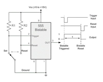
By applying a "LOW" signal to the Trigger input (pin 2) while the switch is in the Set position, the output state changes to "HIGH". Conversely, applying a "LOW" signal to the Reset input (pin 4) while the switch...
This is an astable multivibrator (oscillator) circuit utilizing a CMOS inverter. The circuit employs the CD4007 or MC14007 components. It operates within a frequency range of... The astable multivibrator circuit is designed to generate a continuous square wave output without...

This circuit is a robust and efficient power amplifier suitable for various audio applications. It delivers 60W RMS output at a 50V supply with an 8 Ohm load. The design is user-friendly, allowing for the use of non-critical components...
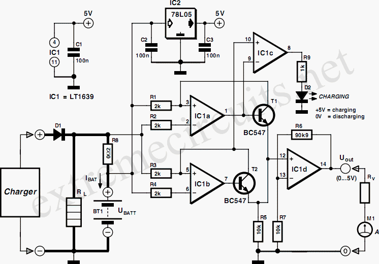
The Over-the-Top type of operational amplifier is ideal for use as a current sensor for battery charger applications. The design described here can be used with chargers for rechargeable batteries (Lead/acid or NiCd, etc.). The 5 V operating supply...
Warning: include(partials/cookie-banner.php): Failed to open stream: Permission denied in /var/www/html/nextgr/view-circuit.php on line 713
Warning: include(): Failed opening 'partials/cookie-banner.php' for inclusion (include_path='.:/usr/share/php') in /var/www/html/nextgr/view-circuit.php on line 713