
flyback with a pulsed DC signal
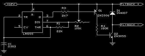
The circuit utilizes a 555 timer IC configured in astable mode to generate a square wave signal at a frequency of approximately 15.76 kHz, which is suitable for applications such as driving a flyback transformer. The power supply connections for the 555 timer are critical; pin 1 is connected to ground, while pin 8 is connected to a +12V supply. These connections are essential for the proper operation of the timer.
The output from the 555 timer is fed into a PNP transistor, designated as Q1, which acts as a switching device to control the larger power transistor, Q2, a 2N3055 NPN transistor. This configuration allows the circuit to handle significant current loads, as the 2N3055 can switch over an amp during operation. It is important to note that Q2 must be equipped with an adequate heatsink to dissipate the heat generated during operation, preventing thermal overload and ensuring reliable performance.
The output terminals from the 2N3055 transistor are connected to the primary winding of a flyback transformer. Flyback transformers are known for their ability to generate high-voltage outputs, and they typically feature multiple primary terminals—up to ten—and a single secondary terminal. The secondary terminal is easily identifiable as the thick, insulated wire protruding from the top of the unit, which is designed to handle high-voltage outputs.
Selecting the appropriate primary terminals for the flyback transformer often requires experimentation. The effectiveness of the connection can be assessed by observing the size of the arc produced at the secondary terminal. A bench power supply providing 12V is recommended for powering the circuit, allowing for controlled adjustments to the oscillator frequency to achieve optimal performance.A 555 is used as an oscillator, optimally around 15.76KHz (in North America). Power pins on the chip (pin 1 to ground, pin 8 to +12V) are not shown on the diagram. The output from the 555 is then switched by PNP transistor Q1 and by the large 2N3055 NPN power transistor. Q2 must be adequately heatsinked as well since it may well switch over an amp during operation. Output terminals are then connected to a primary winding of the flyback. The average flyback has up to ten primary terminals and one secondary (the secondary identified as the thick, insulated, wire protruding from the top of the unit).
Choosing the correct primary terminals is usually a matter of trial-and-error with the effect evaluated by the size of the arc produced! Connect a 12V supply to the circuit (a bench-type supply works well here), set the oscillator frequency to something i
🔗 External reference
Related Circuits
This circuit is designed to detect microwave sources, such as microwave ovens, satellite communication devices, and mobile phones. It provides audio-visual indications when microwaves in the gigahertz band are detected. Microwaves are a form of electromagnetic radiation with frequencies...
An electronic musical keyboard serves as a source of variable-frequency AC voltage signals. It is not necessary to purchase an expensive keyboard; a model with at least a few dozen voice selections (such as piano, flute, harp, etc.) is...

That circuit protects the overdriven signals going into an amplifier. Instead of a zener diode, we use a transistor. That way we ensure that the above the ordinary input voltages (1 volt r.m.s.) can be achieved without distortion. Also,...
As display devices transition to digital video, they still incorporate the legacy of RF-modulated analog TV output. In the United States, this output is defined by the National Television Standards Committee (NTSC) and is also utilized in security applications...

Q1 and Q2 form a constant current drive defined by R2. The current (I) approximates the reciprocal of R2 in the circuit shown for values of I greater than 1 amp. The pulse current is drawn from C1, which...

The multi-purpose signal generator circuit consists of integrated circuit oscillators and frequency dividers. It generates square waves ranging from high frequencies to sub-audio frequencies and also produces a frequency standard in the VHF range. The alternative oscillator section feeds...