
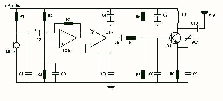
fm antenna booster circuit

The FM antenna booster circuit is designed to amplify weak radio frequency signals received from distant FM stations, improving audio clarity and reception quality. The core component, the 2SC2570 transistor, operates as a common-emitter amplifier, providing significant gain to the incoming RF signals. This transistor is suitable for VHF/UHF applications, making it ideal for FM reception.
The circuit layout should prioritize minimizing interference and ensuring stable operation. The use of a high-quality printed circuit board (PCB) is essential to reduce parasitic capacitance and inductance, which can adversely affect performance. The input and output trimmers (VC1 and VC2) allow for fine-tuning of the circuit to achieve maximum gain, accommodating variations in signal strength and frequency.
Coil L1, with its four turns of 20 SWG enameled copper wire, serves as the input inductor, which is crucial for tuning the circuit to the desired frequency. The spacing of the windings is important for maintaining the coil's inductance and minimizing losses. The tap on L1 enables the circuit to adjust its input impedance, optimizing the signal transfer from the antenna to the amplifier. Coil L2, with three turns, acts as a coupling inductor, further enhancing the signal amplification process.
The pin configuration of the 2SC2570 transistor should be carefully followed to ensure proper connections and functionality. The circuit may also benefit from additional components such as bypass capacitors to stabilize the power supply and improve overall performance. Proper grounding techniques should be employed to minimize noise and improve signal integrity.
In summary, the FM antenna booster circuit is a straightforward yet effective solution for enhancing FM signal reception, making it an excellent project for electronics enthusiasts and professionals alike.This is a low cost fm antenna booster that can be used to listen to program from distant FM stations clearly. The antenna fm booster circuit comprises a common-emitter tuned RF preamplifier wired around VHF/UHF transistor 2SC2570 (C2570).
This is the schematic of the simple FM Antenna Booster. Assemble the circuit on a good quality of printed circ uit board. Adjust input/output trimmers (VC1/VC2) for maximum gain. Input coil L1 consists of four turns of 20SWG enameled copper wire (slightly space wound) over 5mm diameter former. It is tapped at the first turn from ground lead side. Coil L2 is similar to L1, but has only three turns. Pin configuration of transistor 2SC2570 is shown in the fm antenna booster schematic. 🔗 External reference
Related Circuits
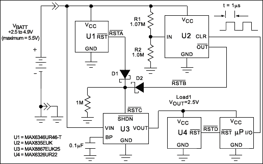
The micropower circuit automatically provides shutdown, power-up, and low-battery lockout functions without requiring software or operator control. The micropower circuit is designed to manage power efficiently in battery-operated devices, ensuring optimal functionality while conserving energy. The shutdown feature is activated...
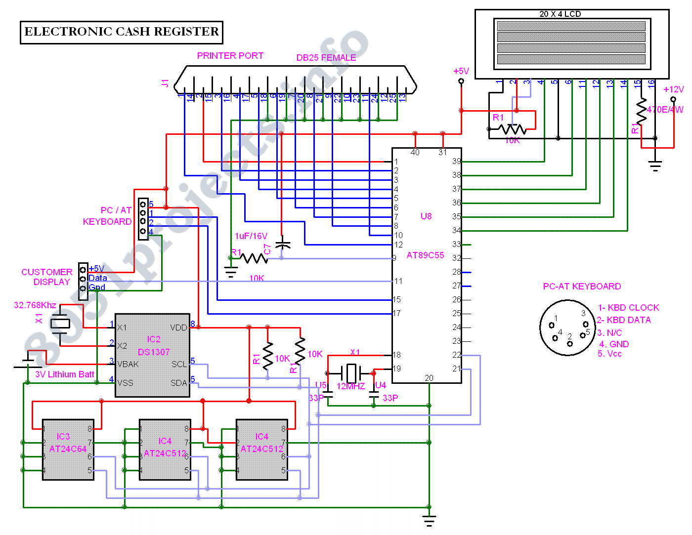
The Electronic Cash Register (ECR) keeps track of sales transactions quickly and effectively. An abundance of PLUs (Price Look Ups) and department keys accommodate a variety of merchandise items. This means a faster, more accurate check out process and...
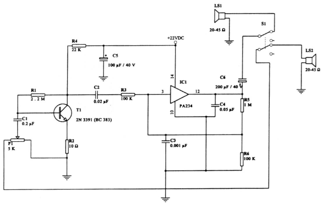
This intercom circuit is versatile and can be utilized in various applications. It operates at 22V, although it may function at a lower voltage (experimental testing is suggested). The circuit utilizes a loudspeaker with an impedance of 20-45 Ohms...
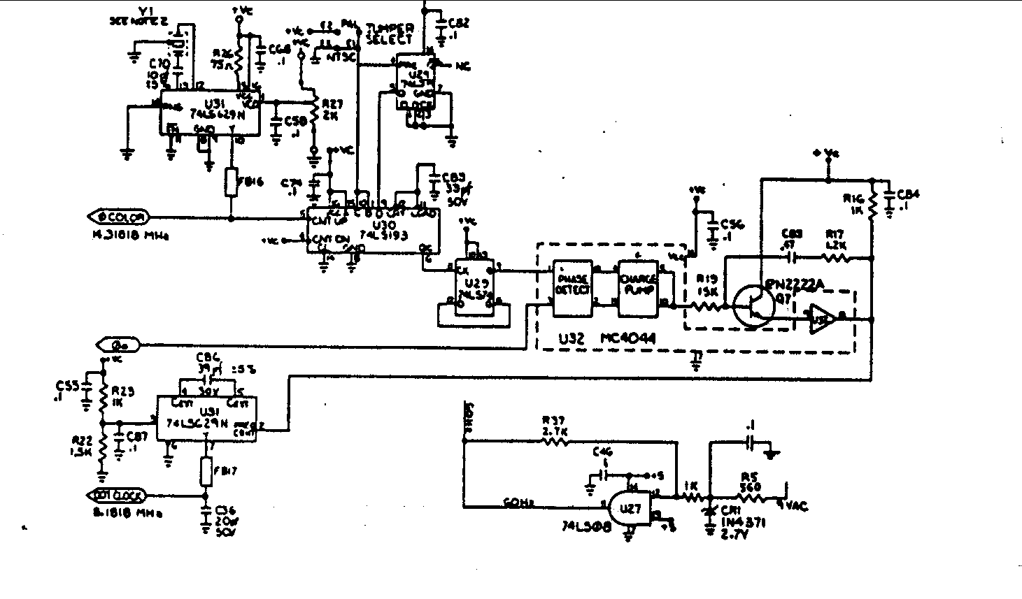
Crystal Y1 generates a fundamental frequency clock signal of 14.31818 MHz. U31 is a Dual Voltage Controlled Oscillator (VCO) that produces a 14.31818 MHz clock signal, referred to as the color clock, at pin 10. The output frequency can...
L1 is 0.112uH (this tunes to the middle of the FM band, 98 MHz, with VC1 at its centre value of 33pF). L1 is 5 turns of 22 swg enamelled copper wire close-wound on a 5mm (3/16") diameter former....
This ultrasonic dog repeller circuit is designed to deter aggressive dogs. It is constructed using the well-known 555 timer circuit, a buzzer, and a small ferrite transformer. The ultrasonic dog repeller circuit operates by emitting high-frequency sound waves that are...